
3D and 2.5 ICS offer a more compact form factor and minimize power consumption compared to traditional packaging methods, which is important for mobile gadgets and other space-constrained applications. The key players operating in the market are focused on adopting inorganic growth strategies like acquisition and merger to develop advance technology for manufacturing 3D IC and 2.5D IC packaging which is estimated to drive the global 3D IC and 2.5D IC packaging market over the forecast period.
3D IC and 2.5D IC Packaging Market: Improve Semiconductor Functionality
The packaging technology of 2.5D and 3D is used to package several integrated circuits in one package. To achieve a very high die-to-die connection density, two or more active semiconductor chips are arranged side by side on a silicon interposer in a 2.5D configuration. Die stacking is used in 3D structures to incorporate active chips for the shortest connectivity and smallest package footprint. 2.5D and 3D have become more and more popular as the best chiplet integration* platforms in recent years because of their advantages in obtaining very high package densities and good energy efficiency.
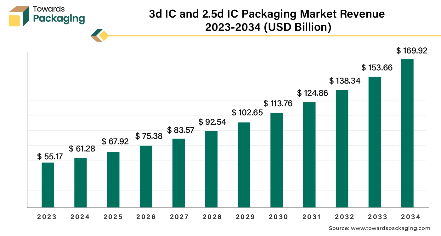
The packaging technology of 2.5D and 3D are cutting-edge methods used to improve semiconductor devices’ efficiency, functionality, and performance. In order to create a three-dimensional structure, many layers of silicon wafers or dies are stacked vertically in 3D IC packaging. Logic, memory, and analogue integrated circuits (ICs) can all be integrated into one package thanks to this stacking. allows for greater capability in a smaller package. Performance is improved via shorter interconnects between layers, which shorten the time a signal travels. It is possible to boost data bandwidth between components by stacking layers.The global 3D IC and 2.5D IC packaging market size reached US$ 55.17 billion in 2023 and is projected to hit around US$ 169.92 billion by 2034, expanding at a CAGR of 10.85% during the forecast period from 2024 to 2033.
How Can AI Improve the 3D IC AND 2.5D IC Packaging Industry?
Artificial Intelligence can help find and create new materials that will improve IC packaging performance and dependability. Artificial Intelligence (AI) can find interesting candidates for novel materials by evaluating performance data and material attributes. The 3D and 2.5D IC packaging sector can achieve better performance, increased efficiency, and improved quality by utilizing AI, which will spur additional innovation and growth in this area.
Increasing Demand for Consumer Electronics
Rapid industrialization and urbanization has given boom to consumer electronics demand and encouraged the development of new gadgets to be used in day-to-day life. Continuous innovation in electronics leads to new and improved devices with enhanced features, performance, and capabilities. This drives consumers to upgrade to the latest technology. The increasing trend of streaming services, gaming, and other digital media expands the demand for high-quality consumer electronics like TVs, audio systems, and gaming consoles. The demand for smartphones, tablets, and other portable devices continues to grow as they become essential tools for communication, work, and entertainment. The proliferation of the Internet of Things (IoT) and smart devices has developed an expanding ecosystem of connected electronics, from smart homes to wearable technology, boosting demand.
Increasing initiatives for smart infrastructure and smart city projects
Due to rapid development in automotive industry and aim to reduce CO2 emission, the electric vehicles are adopted by the most of the people. Smart infrastructure and smart city projects are increasingly becoming a focus for urban development and modernization. Advancing intelligent transportation systems (ITS) to improve traffic management, reduce congestion, and enhance public transportation through real-time data and connectivity.
3D WLCSP to Lead the Market in 2023
The 3D wafer-level chip-scale packaging (WLCSP) segment held a dominant presence in the 3D IC and 2.5D IC packaging market in 2023.
- The 3D wafer-level chip-scale packaging (WLCSP) allows for very compact packaging, that is crucial for modern electronic devices that need smaller and lighter components. By stacking chips vertically, it reduces the distance between components, leading to shorter signal paths and improved performance and speed.
- 3D wafer-level chip-scale packaging (WLCSP) allows integration of advanced cooling techniques, assisting in management of heat more effectively in densely packed circuits. It supports high levels of integration, including combining different types of chips (e.g., logic, memory) in a single package, which is beneficial for complex applications and systems. The short interconnects between chips reduce parasitic capacitance and inductance, improving signal integrity and reducing power consumption and cost of development.
MEMS/Sensors to Show Notable Share in 2023
The MEMS/Sensors segment accounted for a notable share of the 3D IC and 2.5D IC packaging market in 2023. MEMS and sensors often require integration with additional electronic components (e.g., signal processing units, power management circuits). 3D IC and 2.5D IC packaging enable compact, high-density integration, minimizing the overall footprint and supporting for more compact device designs. Microelectronics, microactuators, and microsensors are the functional parts of MEMS.
Asia’s 79% Development in Tech Hub to Support Dominance
Asia Pacific region dominated the global 3D IC and 2.5D IC packaging market in 2023. Asia-Pacific region is home to leading semiconductor manufacturers and foundries, such as Samsung and Taiwan Semiconductor Manufacturing Company (TSMC).
More than 89% of Japan’s GDP is generated by the automobile industry. Japan is actually the third-biggest automobile manufacturer in the world! However, Japan has not embraced zero-emission vehicles (ZEVs) as quickly as several other Asian nations have. Japan’s economic stability will be impacted by the success or failure of its automobile industry as the world transitions more quickly to ZEVs. This will have a big impact on Japan’s still-emerging role in the changing global EV scene.
Technological Leadership in North America to Promote Growth
North America region is projected to host the fastest-growing 3D IC and 2.5D IC packaging market in the coming years. North America, particularly the U.S., is home to major technology and semiconductor companies like Intel, AMD, and NVIDIA, which are leading the development and adoption of advanced packaging technologies, including 3D IC and 2.5D IC. North America has a well-established ecosystem that includes leading packaging technology providers, material suppliers, and equipment manufacturers, which supports the growth and adoption of advanced packaging solutions.
About The Author
Asmita Singh is a renowned author and consultant in the packaging industry, known for her deep passion for knowledge discovery and commitment to delivering actionable insights. With extensive experience in implementing advanced research methodologies, Asmita generates high-quality data and meaningful results that drive innovation and efficiency in packaging solutions. Her expertise spans the globe, offering valuable consulting services to businesses aiming to enhance their packaging strategies. Asmitas work is characterized by a dedication to excellence and a keen understanding of the latest trends and technologies shaping the future of packaging.


