When switching audio and video signals the challenge is doing so without introducing noise, while avoiding signal loss from device resistances or incidental capacitance. While CMOS analog switches are effective and efficient, designers need to be aware of critical parametric trade-offs to apply them correctly.
Switching between audio or video signal sources can be tricky. Most mechanical switches or relays are not designed for switching multimedia signals and can create interference such as a loud audio pop or visual interference. Switching circuits can be designed from scratch, but this adds complexity and time.
To address the problem, simple CMOS analog switches can be used. These act like little semiconductor relays and allow current flow in both directions with low loss. Features such as break-before-make and low on resistance remove audio or visual noise during switching while reducing signal loss.
In practice, however, analog switches carry a trade-off of specifications that designers need to consider before using them. This article will discuss analog switch basics and related design trade-offs before introducing suitable solutions and how to use them.
Analog switch basics
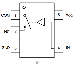
An analog switch uses an N-channel MOSFET in parallel with a P-channel MOSFET to create a bidirectional switch. A simple example of a CMOS analog switch is the NS5B1G384 SPST normally closed analog switch from ON Semiconductor (Figure 1). The control input sends the appropriate inverting and non-inverting signals to the MOSFET gates based on whether the device configuration is normally open (NO) or normally closed (NC).
Ideally, the analog switch should have as low a switch resistance (RON) as possible. This is accomplished by designing the CMOS switch so that the MOSFET drain/source area is larger, creating more surface area for electron flow and reducing the on-state resistance.
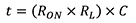
However, increasing the surface area has the drawback of increasing the parasitic capacitance. At higher frequencies, this parasitic capacitance can become an issue by creating a low-pass filter which causes distortion. The capacitor also creates a propagation delay caused by the charge and discharge time of the capacitor. This delay is based on the load resistance and RON, and is given by:
where RL = load resistance.
This trade-off between RON and the parasitic capacitance is key when selecting a CMOS switch for a given application. Not every application requires a low RON, and in some cases the analog switch is in series with a resistive load such that RON is negligible. For video signals, however, the RON verses parasitic capacitance trade-off becomes important. As RON decreases, the parasitic capacitance increases. This cuts off high frequencies resulting in lower bandwidth or distortion.
In the case of the NS5B1G384 shown in Figure 1, this device has a moderately low RON of 4.0 Ω (typical). The parasitic capacitance is a very low 12 picofarads (pF), making the switch applicable for signals up to 330 MHz.
Switching a single audio source
To switch an audio input signal between two audio signal outputs, the audio input is connected to the COM pins of two NS5B1G384 switches. The NC pin of each switch is connected to their respective transducer, such as a headset and a speaker. Note that only one IN pin at a time should be selected.
In this configuration, the turn-on time and the turn-off time of the analog switches becomes important. For the NS5B1G384, the turn-on time is 6.0 nanoseconds (ns) and the turn-off time is 2.0 ns. When using multiple switches, the faster turn-off time provides a break-before-make feature. This ensures one switch is disconnected before another switch is connected, preventing two loads from being connected at the same time. This also reduces the popping sound sometimes heard on audio equipment when switching audio signals.
Switching a differential audio source
An alternate solution to switching between two audio signal outputs is to use two SPDT analog switches. For example, the ADG884BCPZ-REEL from Analog Devices has two SPDT analog switches in one package. With a 5 volt supply, each of the two switches has a very low RON of between 0.28 Ω (typical) and 0.41 Ω (max), making them appropriate for low loss audio signal switching. However, such a low RON comes with a price. The parasitic capacitance between the analog switch contacts when the switch is on is 295 pF.
The ADG884 can handle 400 mA through the switches, making it appropriate to direct drive speakers from an audio amplifier (Figure 2).
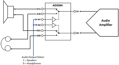
To minimize the possibility of EMI injecting noise into the audio output, the audio amplifier should be positioned as close to the ADG884 as possible on the pc board. The headphone jack should also be as close to the ADG884 as possible. If the speaker does not use a jack, a shielded audio cable should be used between the ADG884 and the speaker.
If the audio input signal is a differential pair, the signal pairs S1A/S1B, S2A/S2B, and D1/D2 should be routed right next to each other on the pc board to cancel out any shared interference, thereby eliminating the noise from the speaker or headphones.
Eliminating audio popping during switching
To further enhance the quality of switched audio signals when using high power amplifiers, shunt resistors should be used to remove any built-up charge at the audio amplifier output. To simplify this, some analog switches have built-in shunt resistors. A good example is the MAX14594EEWL+T DPDT analog switch from Maxim Integrated.
To eliminate the popping sound when switching from an audio amplifier, the MAX14594E has break-before-make operation, and also provides internal shunt resistors to discharge the audio amplifier input coupling capacitors when the switches are opened (Figure 3).
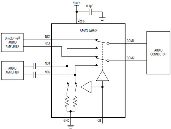
The MAX14594E is a DPDT analog switch and can be used to switch both lines of an audio signal simultaneously using one control input, CB. RON is 0.25 Ω while the parasitic capacitance is 50 pF. Note that compared to the NS5B1G384, RON is much lower, but consequently the parasitic capacitance is much higher.
In reference to Figure 3, CB is pulled low to connect NC1 and NC2 to COM1 and COM2, respectively. At the same time, this connects the output of the audio amplifier at NO1 and NO2 to the shunt resistors. When CB is pulled high, NO1 and NO2 are connected to COM1 and COM2, respectively, which also disconnects the shunt resistors.
The MAX14594E can be controlled by a microcontroller with a GPIO level of 1.8 volts or higher, as CB has a 1.4 volt logic high threshold. Connecting a GPIO pin with a small capacitor of about 0.1 microfarad (µF) between the CB pin and ground will smooth out any transients.
Switching video signals
Things get more complicated when switching video signals as the RON verses parasitic capacitance trade-off becomes important due to the higher frequency signals. Low RON analog switches have a larger parasitic capacitance which reduces bandwidth, and results in reduced video quality.
As such, using higher RON analog switches with their correspondingly lower parasitic capacitance is recommended for video switching. However, this decreases the video signal amplitude which must be compensated for by adding additional video amplifiers. As multiple high frequency signals may need to be switched at once, it’s important to have a circuit board design that is as compact as possible to avoid signal loss. To help meet this objective, selecting analog switches that are highly integrated is essential.
For example, the QS4A110QG from Integrated Device Technology (IDT) is a dual 5PST analog switch that targets high speed video signal switching applications. It has a moderately low RON of 5 Ω and an extremely low parasitic capacitance of 10 pF, enabling a bandwidth of 1.8 GHz (Figure 4).
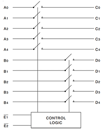
Looking at Figure 4, it can be easily converted to a single 5PDT by connecting the A(x) and B(x) signals to each other so that the switched outputs are either C or D. As both control signals E1# and E2# are active low, a logic signal connected to one control signal with an inverter and to the other control signal with a noninverting buffer, allows for output selection. While the noninverting buffer is optional, it is good practice to include it to prevent a race condition between the switch outputs.
The QS4A110 has a turn-on time of 6 ns and turn-off time of 6.5 ns (max). As such, the turn-on and turn-off times in a circuit are effectively the RC delay of the switch and load capacitance.
Conclusion
Analog switches appear easy to design into a circuit, but they are not one size fits all. Their trade-off of lower RON and higher parasitic capacitance, or higher RON and lower parasitic capacitance directly affects their bandwidth. Selecting the device that has the proper characteristics for the target design is paramount.


