
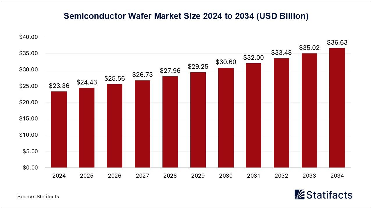
The global semiconductor wafer market size is predicted to gain around USD 36.63 billion by 2034, growing from USD 23.36 billion in 2024, at a CAGR of 4.6% from 2025 to 2034. This steady expansion is driven by continuous advancements in semiconductor manufacturing processes, the rising adoption of electric vehicles (EVs), and the surging demand for high-performance computing.
In the rapidly advancing world of technology, semiconductor wafers play a pivotal role in shaping the future of electronic devices. These thin slices of semiconductor material serve as the foundation for microchips, integrated circuits, and a vast range of electronic components. As the demand for smaller, more efficient, and powerful devices increases, innovations in semiconductor wafer technology are becoming more crucial than ever.
What is a Semiconductor Wafer?
A semiconductor wafer is a thin slice of semiconductor material, typically silicon, that acts as a substrate for the fabrication of microelectronic circuits. The process of creating a wafer involves several complex steps, including crystal growth, slicing, polishing, and doping, which influence the electrical properties of the final product.
Silicon is the most commonly used material due to its abundance, cost-effectiveness, and excellent electrical properties. However, other materials such as gallium arsenide (GaAs) and silicon carbide (SiC) are also used in specific applications, particularly in high-power and high-frequency devices.
The Manufacturing Process
- Crystal Growth
The process begins with the growth of a pure silicon crystal using the Czochralski (CZ) method. A silicon seed crystal is dipped into molten silicon and slowly pulled upward while rotating to form a cylindrical single-crystal ingot.
- Wafer Slicing
The ingot is sliced into thin wafers using precision saws, ensuring uniform thickness. These wafers undergo initial shaping to remove any surface irregularities.
- Polishing and Cleaning
The wafers are polished to achieve a mirror-like surface, which is essential for high-performance microchip fabrication. After polishing, rigorous cleaning is performed to eliminate contaminants that could impact the semiconductor’s performance.
- Doping and Oxidation
To modify the electrical properties, wafers are doped with elements such as phosphorus or boron. This process is followed by oxidation, where a thin insulating layer of silicon dioxide is formed on the wafer’s surface to enhance its functionality.
Applications of Semiconductor Wafers
The importance of semiconductor wafers extends across various industries, including:
- Consumer Electronics – Used in smartphones, laptops, televisions, and gaming consoles.
- Automotive Industry – Essential for advanced driver-assistance systems (ADAS), electric vehicles (EVs), and infotainment systems.
- Telecommunications – Integral to the production of high-speed communication devices, 5G networks, and satellite technology.
- Healthcare – Found in medical imaging devices, wearable health monitors, and biomedical sensors.
- Industrial & Defense – Used in automation, aerospace, and defense applications for high-performance computing and radar systems.
Advancements in 5G Technology Driving Growth in the Semiconductor Wafer Market
The rapid evolution of 5G technology within the telecommunications sector is significantly boosting the demand for semiconductor wafers. With enhanced speeds, reduced latency, and the ability to support a vast number of connected devices, 5G technology requires semiconductors that can operate at higher frequencies and process data at unprecedented speeds.
Leading companies in the industry are developing advanced semiconductor materials, such as SK Siltron Neveon’s silicon carbide (SiC) and gallium nitride (GaN) wafers, to support next-generation semiconductor devices. These materials are particularly well-suited for 5G applications due to their superior power-handling capabilities and high-frequency performance.
Key growth opportunities in the market include the production of wafers for 5G base stations and network infrastructure. Since these components must process vast amounts of data with exceptional speed and reliability, the demand for high-performance wafers with consistent quality is rising. As telecom providers worldwide continue expanding their 5G networks, the need for specialized semiconductor wafers is surging, further driving industry growth.
Future Trends in Semiconductor Wafer Technology
The semiconductor industry is evolving rapidly, with several trends shaping its future:
- Miniaturization & Moore’s Law – The continuous drive to create smaller, more powerful chips is pushing innovation in wafer manufacturing, leading to advancements in extreme ultraviolet (EUV) lithography.
- Advanced Materials – Researchers are exploring compound semiconductors like GaN (gallium nitride) and SiC for high-efficiency applications.
- 3D Stacking & Chiplets – Instead of a single monolithic chip, manufacturers are focusing on stacking multiple layers of semiconductor wafers for enhanced performance and efficiency.
- Sustainability Initiatives – The semiconductor industry is working towards reducing waste and improving energy efficiency in wafer production processes.
Technological Complexity and Environmental Concerns to Hinder Semiconductor Wafer Market Growth
The semiconductor wafer market faces significant challenges due to the relentless demand for smaller, faster, and more cost-effective chips. As semiconductor technology advances, wafer fabrication becomes increasingly intricate, requiring precise control over complex processes such as lithography, etching, and deposition. The ongoing trend toward shrinking node sizes reaching 5nm and below further exacerbates this complexity. Maintaining high yield rates and ensuring defect-free wafers demand continuous technological advancements and sophisticated manufacturing expertise.
Additionally, environmental concerns present another major restraint in the market. Wafer production is highly energy-intensive, relying predominantly on non-renewable energy sources, which contributes to increased carbon emissions. Furthermore, the use of hazardous chemicals including acids, solvents, and gases poses significant health and environmental risks. In response, governments worldwide are implementing stringent regulations to promote sustainable manufacturing practices. Consequently, semiconductor manufacturers are investing in eco-friendly initiatives, such as reducing energy consumption and minimizing waste. However, these green initiatives often lead to increased production costs, posing further challenges for market players.
Country-wise Insights
Increasing Demand for Consumer Electronics Devices is Boosting Semiconductor Wafers Market Growth in the USA
The Semiconductor Industry Association (SIA) highlights that the USA holds a significant share of the global semiconductor industry. The rising consumer demand for smart appliances is further driving growth, prompting manufacturers in the consumer electronics sector to expand their production facilities. Semiconductor wafers, essential for integrated circuits, play a crucial role in enhancing the functionality and efficiency of these appliances.
The USA currently dominates the North American semiconductor wafer market, and industry trends indicate that this leadership position is expected to continue in the coming years. The market is projected to experience steady growth throughout the forecast period.
Rapid Industrialization and Technological Advancement Propelling the Market in China
China’s semiconductor wafer market is expanding as companies prioritize technological advancements to accelerate digitization. A significant portion of global semiconductor patents originates from China, reflecting the country’s commitment to innovation. Companies in this region are developing advanced technologies to enhance the flexibility and operational efficiency of semiconductor devices.
Additionally, the surge in smart factory construction is further contributing to market expansion. China currently holds the largest share of the East Asian semiconductor wafer market, and this trend is expected to persist well into the future.
Supportive Government Initiatives for the Semiconductor Industry in India Creating a Positive Market Outlook
India’s semiconductor wafer market is on a strong growth trajectory, driven by significant government investment in the sector. The Indian government is actively supporting the semiconductor industry to boost economic growth and reduce reliance on foreign technology.
A recent government initiative allocated substantial funding for the construction of semiconductor fabrication facilities. These fabs will have a considerable production capacity and focus on manufacturing mature chip technologies, reinforcing India’s position in the South Asia & Pacific markets.

 Market Size to Cross USD 2,701.74 Mn by 2034")


