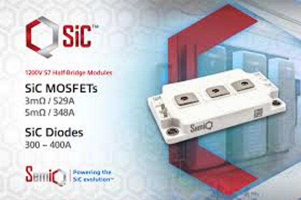
The high-performance 1,200V SiC power modules offer optimized solutions for new designs and improved performance in legacy applications.
SemiQ Inc has added a new S7 packaging to its QSiC family of SiC power modules, which consists of 1,200V, half-bridge MOSFET and Schottky diode modules. The components provide power engineers with increased design flexibility by offering compact, high-efficiency, and high-performance choices for new designs. They also facilitate the seamless replacement of older systems that require improved efficiency.
The latest announcement includes the release of four new electronic modules: a 529A MOSFET module (GCMX003A120S7B1), a 348A MOSFET module (GCMX005A120S7B1), and two low-noise SiC Schottky diode half-bridge modules (GHXS300A120S7D5 and GHXS400A120S7D5). These modules come in a S7 package with industry-standard 62.0 mm footprints and a height of 17.0 mm.
The new package caters to the specific size, weight, and power needs of various demanding applications, including induction heaters, welding equipment, uninterruptible power supplies (UPS), photovoltaic and wind inverters, energy storage systems, high-voltage DC-DC converters, and battery charging systems for electric vehicles (EVs). In addition to the tiny size of the modules, their high efficiency and low-loss operation minimize heat dissipation in the system and enable the use of smaller heatsinks.
SemiQ’s objective is to offer a wide range of SiC technologies that enable designers to enhance the efficiency, performance, and size of current demanding applications. The introduction of a new packaging option for the 1,200V QSiC MOSFET and SiC diode module families expands the range of alternatives for designers seeking to develop novel applications or enhance existing systems without the need for extensive redesign.
SemiQ’s modules are made from high-performance ceramics, which enable them to achieve outstanding performance levels. These modules also offer higher power density and allow for more compact designs, particularly in high-frequency and high-power settings.
To ensure a consistent gate threshold voltage and high-quality gate oxide for every module, SemiQ performs gate burn-in testing at the wafer level. Aside from the burn-in test, which helps reduce external failure rates, several stress tests are used to achieve the required quality standards for automotive and industrial applications. These stress tests include gate stress, high-temperature reverse bias (HTRB) drain stress, and high humidity, high voltage, high temperature (H3TRB). All components have undergone testing that exceeds 1,400 volts.


