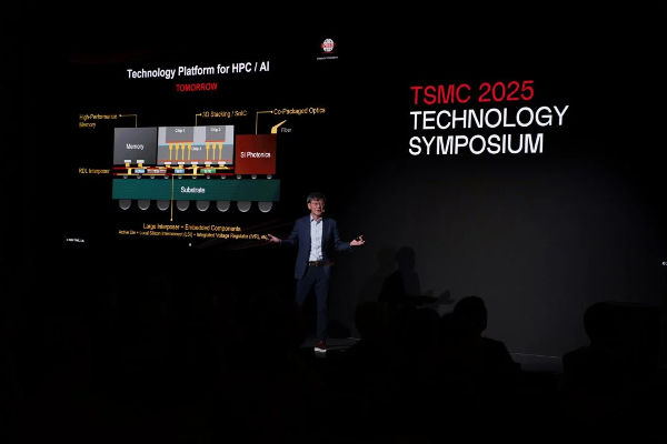
Taiwanese chipmaker (TSMC) is set to open its first European design center in Munich, focusing primarily on automotive technology. The new European Union Design Center (EUDC), scheduled to open in Q3 2025, will also support development in industrial, AI, telecom, and IoT applications. It will join TSMC’s global network of nine other design centers across Taiwan, the U.S., Canada, China, and Japan.
To meet the demands of next-generation automotive electronics, TSMC is pushing forward with advanced memory technologies. It has already qualified 28nm RRAM (resistive RAM) for automotive use, with 12nm and 6nm versions in the pipeline. In parallel, TSMC is advancing its MRAM (magnetoresistive RAM) roadmap, with 22nm in production, 16nm ready for customer deployment, and 12nm under development. Notably, the company is also exploring MRAM and RRAM scalability down to 5nm and 6nm nodes, respectively—an important step for automotive ADAS and AI systems.
At its Technology Symposium in Amsterdam, TSMC highlighted several automotive innovations, including AI-focused power management, high-dynamic-range image sensors for varying lighting conditions, and advanced packaging for smart vehicles. The company expects to qualify its 3nm process for automotive applications later in 2025, enabling the production of high-performance AI and ADAS chips.
For IoT, TSMC is working on an experimental 4nm (N4e) process to lower operating voltage below 0.4V, along with ultra-low-leakage SRAM and logic for extended battery life.
TSMC’s 3nm platforms (N3, N3E, N3P, and N3A) are progressing well, with over 70 tapeouts as of April 2025. The N3A node, designed for automotive-grade chips, is on track for qualification and production by the end of 2025.
Looking ahead, TSMC forecasts that automotive chips will make up 15% of the $1 trillion semiconductor market by 2030, compared to 10% for IoT. AI and datacenter technologies are expected to dominate, accounting for 45% of the market. To support this, TSMC plans to start construction on Fab 25 in Taichung, Taiwan, later this year, targeting future A14 and A16 process technologies using advanced CFET (complementary FET) designs for higher transistor density.
In the display space, TSMC unveiled the industry’s first FinFET high-voltage platform for applications like foldable OLEDs and AR glasses. Its 16HV technology offers 28% power savings and 41% increased logic density compared to 28HV.


