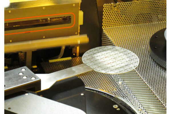
WIN Semiconductors has announced the launch of its new 0.12μm gate-length depletion-mode GaN HEMT technology, NP12-1B, built on silicon carbide (SiC) substrates and set for high-volume production in Q3 2025. This advanced process targets high-power applications across K-Band to V-Band frequencies and operates at 28V, making it suitable for demanding RF and microwave systems.
The NP12-1B process features several key transistor enhancements, including a source-coupled field plate design that enables a typical gate-to-drain breakdown voltage of 120V. This supports high power density, better linearity, and reliable performance in high-compression continuous wave (CW) scenarios.
Designed for use in high linearity amplifiers, NP12-1B is optimized for a wide range of applications such as mmWave and microwave communication systems, radar (airborne, shipborne, and ground-based), electronic warfare, avionics, wireless infrastructure, ultra-wideband and broadband systems, as well as test and measurement equipment. Its strong linearity performance is crucial for minimizing distortion and maintaining signal clarity in crowded frequency environments.
The technology is backed by a full Process Design Kit, including large-signal and small-signal models, and comes with a qualification report upon request. An optional moisture-resistant version is also available, providing enhanced reliability for plastic-packaged devices.


