
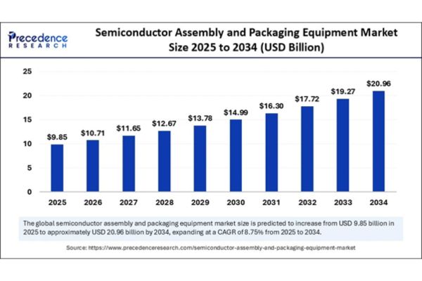
According to Precedence Research, the global semiconductor assembly and packaging equipment market size is expected to surge around USD 20.96 billion by 2034 from USD 9.06 billion in 2024, at a CAGR of 8.75%.
Semiconductor Assembly and Packaging Equipment Market Key Insights
- Asia Pacific held the dominant position in 2024, accounting for 75% of the total market share.
- Based on equipment type, the die attach equipment segment accounted for the largest share of the market in 2024, contributing 25% to the total revenue.
- The flip chip bonders / advanced die bonders segment is forecasted to register the fastest growth rate among equipment types throughout the forecast period.
- By packaging type, the wire bond packaging segment led the market in 2024.
- The flip chip packaging segment is projected to grow at an impressive CAGR of 15% from 2025 to 2034.
- In terms of application, consumer electronics emerged as the leading segment in 2024.
- The automotive electronics segment is expected to witness rapid expansion, with a projected CAGR of 20% between 2025 and 2034.
- Among end-users, OSAT (Outsourced Semiconductor Assembly and Test) companies held the largest market share in 2024.
- The foundries segment is poised to experience significant growth during the forecast period.
How is AI Transforming the Semiconductor Assembly and Packaging Equipment Market?
Artificial Intelligence (AI) is playing a pivotal role in revolutionizing the semiconductor assembly and packaging equipment market by driving automation, precision, and efficiency across manufacturing processes. AI-powered systems are being integrated into assembly and inspection equipment to enable real-time defect detection, predictive maintenance, and adaptive process control. These advancements significantly reduce downtime, minimize human error, and improve overall production yields, which is critical for meeting the growing demand for high-performance semiconductor devices.
Moreover, AI is enhancing the design and optimization of packaging architectures, particularly in advanced packaging methods like flip-chip and 3D stacking. By analysing massive datasets and simulating various process parameters, AI helps engineers make faster and smarter decisions, leading to shorter development cycles and lower costs. As semiconductor devices become smaller and more complex, the adoption of AI across packaging and assembly lines is expected to become a competitive necessity rather than a mere innovation.
Regional Outlook of Semiconductor Assembly and Packaging Equipment Market
Asia Pacific
Asia Pacific remains the dominant region in the semiconductor assembly and packaging equipment market. This strength is underpinned by its robust manufacturing ecosystem in countries such as China, Taiwan, South Korea, and Japan, all of which offer well-established infrastructure and skilled labor essential for large-scale chip production. Vertically integrated supply chains in the region help reduce costs and turnaround times.
Massive investments in advanced electronics, 5G, AI, and electric vehicles continue to fuel demand for sophisticated packaging solutions. Further, government incentives and aggressive innovations in packaging by local firms keep the region at the industry forefront. India is also emerging as a key contributor with favorable policies, while Vietnam is rapidly growing as a preferred manufacturing base due to its cost advantages and supportive industrial strategies.
North America
In North America, the market is witnessing high growth, driven by increased R&D investments, accelerated adoption of AI and smart technologies, and a significant push to reshore semiconductor production. The U.S. leads the region through its focus on building advanced packaging facilities, supported by federal initiatives like the CHIPS and Science Act.
This is complemented by a strong ecosystem for developing 3D ICs, chiplet integration, and advanced thermal management systems. North America’s market is characterized by high-value, low-volume production—especially for defense, aerospace, and other mission-critical applications. Collaborative efforts among academia, industry, and government continue to foster innovation and bolster resilience against global supply chain risks.
Europe
Europe’s market for semiconductor assembly and packaging equipment is bolstered by a robust automotive and industrial electronics sector, which demands high-reliability packaging technologies. The region is an active adopter of fan-out and 2.5D packaging, with strong support from
EU initiatives aimed at increasing semiconductor self-sufficiency. Major investments are being directed toward enhancing die bonding, molding, and advanced system integration equipment, especially by large integrated device manufacturers (IDMs) and specialized OSAT providers.
Middle East & Africa
The Middle East and Africa are at an early stage of developing their semiconductor ecosystems. Nevertheless, momentum is building as governments encourage investments in electronics assembly and packaging infrastructure. Growth here will depend on market participants supporting global supply chain resilience and localized electronics production.
Latin America
Latin America is gradually emerging as a market for semiconductor assembly and packaging equipment, led by growing investments in local electronics manufacturing. While the region currently plays more of a support role, demand is increasing particularly for entry-level assembly and packaging equipment, with Brazil showing notable progress due to increased government incentives and a rising electronics sector.
Semiconductor Assembly and Packaging Equipment Market Key Trends
1. Rise of Advanced Packaging & Heterogeneous Integration
Technologies such as 2.5D/3D ICs, fan‑out wafer‑level packaging (FOWLP), and system‑in‑package (SiP) are rapidly gaining traction. These advanced techniques enable higher density, better performance, and improved thermal and signal integrity—critical for AI, HPC, and mobile devices. Manufacturers are investing in precision bonding tools to support ultra-fine pitches and multi-chip stacking.
2. AI-Driven Automation, Inspection, and Process Optimization
AI, machine‑vision, and robotics are being deployed across packaging and inspection equipment to enable real‑time defect detection, adaptive process control, and predictive maintenance. These capabilities significantly boost yield, reduce downtime, and enhance throughput—especially important for complex packaging flows.
3. Miniaturization, High-Volume & Precision Equipment Needs
The proliferation of high-performance, miniaturized devices—especially in consumer wearables, 5G, and IoT—drives demand for ultra-thin, compact packaging and sub-5 nm process support. Equipment must handle delicate structures at scale, with high accuracy and minimal variation.
4. Automotive & AI Applications Fuel Specialty Packaging Growth
Automotive electronics and AI/HPC chips are pushing requirements for highly reliable, thermally robust packaging. Automotive semiconductors must endure harsh environments and meet stringent standards, while AI chips require dense interconnects like HBM, driving investment in hybrid bonding and high-end flip-chip equipment.
5. Localisation, Strategic Partnerships & Sustainability
Governments worldwide are incentivizing domestic semiconductor assembly and packaging infrastructure—spurred by geopolitical tensions and the need for supply chain resilience. Companies are forming local partnerships and joint ventures, particularly in Southeast Asia, India, and North America. At the same time, there’s growing emphasis on eco‑friendly materials, lead‑free soldering, and recyclable packaging processes.
6. Strategic Collaborations & R&D Investment
OEMs are cooperating closely with foundries and OSATs to co-develop advanced packaging lines and integrate tools directly into chip architectures. Over 60% of procurement decisions now involve alliances or joint ventures. R&D spending especially in AI-enabled assembly tools is rising to support next-gen capabilities.
Leading Companies in the Semiconductor Assembly and Packaging Equipment Market
- ASMPT (ASM Pacific Technology): Major supplier of advanced assembly and packaging equipment, especially for high-density, miniaturized chip packaging and automation.
- Kulicke & Soffa (K&S): Key player in wire bonding and die attach equipment, enabling both traditional and advanced chip packaging techniques for global chipmakers.
- BE Semiconductor Industries (Besi): Specializes in die/wire bonding and automation, serving applications in 5G, automotive, and AI.
- DISCO Corporation: Leading provider of wafer thinning, dicing, and singulation equipment for chip preparation.
- Tokyo Electron (TEL): Supplies advanced wafer processing and some back-end packaging tools to support new packaging formats.
- Applied Materials: Focuses on hybrid bonding, wafer-level integration, and process innovation for next-gen 3D and heterogeneous semiconductor packaging.
- Onto Innovation (incl. Rudolph Technologies): Delivers inspection and metrology equipment essential for quality control in advanced packaging processes.
- EV Group (EVG): Supplies wafer bonding/lithography tools for 3D and hybrid chip integration scenarios.
- SUSS MicroTec: Provides solutions for temporary bonding, 3D integration, and microstructuring, aiding the shift to more complex chip designs.
- Hanmi Semiconductor: Supplies sawing, placement, and molding systems crucial for back-end chip assembly.
- Shibaura Mechatronics (Toshiba): Produces cleaning and bonding tools for both front- and back-end processes.
- Hitachi High-Tech: Focuses on metrology and inspection equipment enhancing chip production quality.
- Toray Engineering: Develops panel-level and ultra-thin packaging equipment for high-performance servers and similar uses.
- Panasonic Factory Solutions: Provides smart factory automation and process control solutions for semiconductor assembly lines.
- Nidec Sankyo: Specializes in high-precision transfer and automation robotics for wafer and glass handling.
- Intel & Samsung: Lead as major innovators and investors in advanced packaging technologies and collaborate closely with equipment suppliers.
- Amkor Technology: One of the largest OSATs, heavily engaged in the deployment and development of new packaging equipment and technologies.
- Startups in Hybrid Bonding & 3D-IC: Pioneer new packaging methods like hybrid bonding and chiplet integration, often collaborating with larger players to accelerate innovation.
Segmental Insights of Semiconductor Assembly and Packaging Equipment Market
Equipment Type Insights
Die Attach Equipment led the market in 2024. This segment is critical for nearly all chip packages since it places and secures the semiconductor die onto substrates. Its dominance is driven by massive demand in automotive and consumer electronics, where reliability and precision are paramount.
Flip chip and advanced die bonder types are growing fastest, fueled by the need for miniaturization, multi-die stacking, and high-performance applications, especially in AI and 5G fields.
Packaging Type Insights
Wire Bond Packaging held the largest share in 2024 due to its maturity, reliability, and affordability, making it widespread in analog, MEMS, and power devices. Despite being traditional, ongoing innovations (wire materials, automation) are sustaining growth.
Flip chip packaging is projected to see the fastest growth rate thanks to its support for higher I/O density, thermal efficiency, and the demands of AI and high-end computing devices.
Application Insights
Consumer Electronics was the dominant application segment in 2024. The surge in smartphones, wearables, and smart home devices created persistent demand for precision chip packaging. The shift to thinner, multifunctional devices further accelerates needs for both traditional and advanced packaging.
Automotive electronics is the fastest-growing segment, propelled by electric vehicles (EVs), ADAS, and connectivity features that require highly reliable, robust, and high-density semiconductor packaging.
End User Insights
OSAT (Outsourced Semiconductor Assembly and Test) Companies led the market. These firms cater to fabless semiconductor clients with high-volume, cost-effective assembly services across a broad spectrum of package types.
OSATs invest heavily in advanced tools and automation to stay ahead in innovation and efficiency. Foundries, meanwhile, are growing rapidly as they bring advanced packaging operations in-house, blending wafer fabrication with packaging for integrated solutions.


