
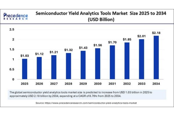
According to Precedence Research, the semiconductor yield analytics tools market is projected to grow from USD 1.03 billion in 2025 to USD 2.18 billion by 2034, at a robust CAGR of 8.76%. This surge reflects the industry’s response to rising chip complexity, the push for higher yields, and the integration of artificial intelligence (AI) and machine learning (ML) in manufacturing workflows.
With advanced nodes, EUV lithography, and chiplet-based architectures becoming mainstream, traditional process-control methods alone can no longer keep pace. Yield analytics tools are increasingly central to identifying hidden defect patterns, optimizing wafer fabrication, and cutting costly variances that hamper profitability.
Quick Insights
- Market Size: USD 1.03 billion (2025) → USD 2.18 billion (2034)
- CAGR (2025–2034): 8.76%
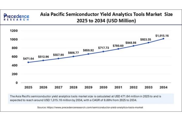
- Top Region (2024): Asia Pacific – 46% market share
- Fastest-Growing Region: North America (2025–2034)
- Leading Tool Type (2024): Yield management software
- High-Growth Tool Segment: Data analytics platforms
- Top Application: Wafer fabrication – 45% share in 2024
- High-Growth Application: Process optimization
- Leading End User: Semiconductor foundries – 50% share in 2024
How Is Artificial Intelligence Transforming Semiconductor Yield Analytics?
As semiconductor devices shrink and wafer fabrication becomes more complex, traditional statistical process-control methods fall short. This is where AI-driven yield analytics is making a profound difference.
AI and ML models help manufacturers:
- Detect micro-defects in real-time before they propagate into large-scale yield loss.
- Predict variance levels caused by contaminants—an issue costing the industry billions annually.
- Optimize wafer quality and prevent downtime through predictive maintenance.
A notable example is Synopsys’ AI Copilot, launched with Microsoft and Azure OpenAI, which supports semiconductor design and yield optimization.
By embedding intelligence into yield management, fabs gain a “digital crystal ball” to foresee potential breakdowns, accelerate time-to-market, and reduce wastage.
Semiconductor Yield Analytics Tools Market Coverage
| Report Attribute | Details |
| Market Size by 2034 | USD 2.18 Billion |
| Market Size in 2025 | USD 1.03 Billion |
| Market Size in 2024 | USD 0.94 Billion |
| Market Growth Rate from 2025 to 2034 | CAGR of 8.76% |
| Dominating Region | Asia Pacific |
| Fastest Growing Region | North America |
| Base Year | 2024 |
| Forecast Period | 2025 to 2034 |
| Segments Covered | Tool Type, Component, End User, Application, and Region |
| Regions Covered | North America, Europe, Asia-Pacific, Latin America, and Middle East & Africa |
Why Is Asia Pacific the Powerhouse of Semiconductor Yield Analytics?
Asia Pacific has cemented its position as the global leader in semiconductor yield analytics tools, accounting for 46% of the market share in 2024. This dominance is set to continue, with the region projected to surpass USD 1 billion by 2034. The foundation of this leadership lies in the region’s unique blend of concentrated manufacturing capacity, strong government policies, and rapid adoption of advanced technologies like EUV lithography and chiplet-based designs.
Country-Wise Insights
- China
- China remains at the forefront with massive state-backed investments into semiconductor independence. Its push for self-reliant chip ecosystems under initiatives like “Made in China 2025” has accelerated demand for yield analytics tools to enhance wafer production efficiency. Chinese fabs are heavily integrating AI-driven analytics to minimize defect rates as they advance toward 28nm and sub-14nm nodes.
- Taiwan
Home to global foundry giants such as TSMC, Taiwan is a key contributor to Asia Pacific’s yield analytics market. The country’s leadership in advanced nodes (3nm and below) requires ultra-precise defect detection and predictive analytics. With TSMC’s continued expansion into high-performance computing and AI chips, Taiwan’s adoption of yield analytics platforms is not just strategic—it’s mission-critical. - South Korea
South Korea’s semiconductor industry, led by Samsung Electronics and SK Hynix, is investing aggressively in yield analytics tools to boost memory and logic production. The country’s focus on DRAM and NAND flash innovation makes yield optimization essential, given the cost sensitivity of the memory segment. South Korea is also embracing EUV lithography faster than most markets, making analytics indispensable for managing variability. - India
India is emerging as a new contender in the region, supported by the Semicon India Program. While still in early stages of semiconductor manufacturing, India is focusing on chip design and testing ecosystems, where yield analytics tools are vital for validation. The government’s drive to establish domestic fabs by the early 2030s signals future growth potential in analytics adoption.
Segmentation Insights
Which Tool Types Are Driving the Market Forward?
The yield management software segment led the semiconductor yield analytics tools market in 2024, supported by its deep penetration in high-volume fabs. As device geometries shrink, these software platforms provide fabs with advanced defect detection, real-time wafer monitoring, and performance optimization. Meanwhile, data analytics platforms are emerging as the fastest-growing category. Their ability to handle massive datasets and apply AI-driven predictions enables fabs to make real-time decisions, marking them as the future powerhouse of yield analytics adoption.
Why Is Software Outpacing Services in Component Growth?
The software segment dominated the market in 2024 and will continue to expand as fabs increasingly adopt digital-first solutions to streamline operations. Integrated software platforms are becoming indispensable in managing yield variability and enhancing production efficiency. However, services are carving out a stronger role as fabs demand expertise in system integration, consulting, and managed analytics. This growing reliance on services ensures that deployment, customization, and workforce training keep pace with rising technological complexity.
Where Are Yield Analytics Tools Most Impactful in Application?
Wafer fabrication accounted for nearly 45% of global market share in 2024, reflecting the segment’s high capital intensity and the urgent need for yield optimization. Even slight improvements at this stage can significantly reduce costs and wastage. On the other hand, process optimization is expected to witness rapid growth, as fabs increasingly prioritize minimizing downtime and leveraging predictive analytics. Tools that can model process scenarios and prevent unexpected failures are becoming essential in ensuring long-term efficiency.
Which End Users Are Leading Adoption Trends?
Semiconductor foundries represented the largest end-user group in 2024, holding roughly 50% of the market. Foundries depend heavily on yield analytics to improve wafer quality and maintain efficiency while serving multiple fabless clients. However, the fastest growth is projected among fabless companies, which are adopting analytics solutions to strengthen collaboration with foundries. By leveraging yield insights during the design and prototyping phase, fabless firms can achieve smoother product launches and better alignment with evolving process technologies.
Opportunity: Is Advanced Process Control the Next Frontier?
Combining advanced yield analytics tools with cutting-edge process control (APC) is emerging as the next major growth avenue. As chip design tolerances narrow at sub-3nm nodes, micro-level monitoring and real-time process adjustments will transform throughput and waste management. Top innovators like TSMC and Applied Materials showcase this trend by investing in advanced metrology systems (SEMVision H20 and more) that deliver nanoscale defect detection for next-generation logic chips.
Expert View
“The next frontier of semiconductor manufacturing is not just about building smaller transistors—it’s about making smarter decisions at every step of the process. Yield analytics powered by AI and ML gives fabs the ability to move from reactive problem-solving to predictive, preventive optimization. This shift will redefine competitive advantage in the chipmaking industry over the next decade.”
— Dr. Maya Verma, Principal Consultant, Precedence Research
Industry Updates: Who Is Leading the Way?
- Synopsys – Expanded AI-driven yield optimization capabilities through strategic collaborations with Microsoft and Azure OpenAI, bringing next-generation analytics into semiconductor design and manufacturing.
- KLA Corporation – Pioneering inspection and metrology systems that integrate with analytics platforms for advanced defect detection and real-time monitoring.
- Applied Materials – Investing in next-generation yield platforms embedded directly into fabrication equipment, ensuring tighter integration of analytics with manufacturing.
- ASML – Strengthening EUV yield-enhancement ecosystems in partnership with top global foundries, enabling better management of advanced lithography complexities.
- Cadence Design Systems – Advancing analytics through design-technology co-optimization (DTCO) platforms that help fabless companies align more closely with foundry requirements.
- Lam Research – Enhancing process control through integrated equipment and analytics tools, helping fabs reduce process variability at the atomic scale.
- Advantest Corporation – Developing test and measurement solutions integrated with analytics for faster identification of wafer and die-level yield issues.
- Hitachi High-Tech – Delivering precision inspection and defect analysis systems that integrate seamlessly into fab-wide yield management platforms.
- Onto Innovation – Expanding its portfolio of process control and yield optimization solutions, particularly for advanced packaging and heterogeneous integration.
- Tokyo Electron (TEL) – Strengthening analytics-driven solutions embedded in etch and deposition equipment, aimed at improving process reliability and throughput.


