
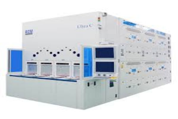
Applied Materials has announced that SCREEN Semiconductor Solutions has become the newest innovation partner at the EPIC Center. Through this collaboration, SCREEN SPE will combine its wafer cleaning technology expertise with Applied Materials’ strengths in materials engineering to create optimized process solutions for next-generation semiconductor chips.
As semiconductor devices have become increasingly complex, precise wafer surface cleanliness has become a critical enabler of yield, device performance, and reliability at the most advanced process nodes. Any defects introduced during deposition, etch, and materials modification steps must be addressed with ever-greater precision, making co-optimized cleaning solutions an essential component of developing next-generation materials engineering technologies.
By combining Applied’s deep process expertise across deposition, dry etch and materials modification with SCREEN SPE’s industry-leading cleaning, wet etch and surface preparation capabilities, the two companies can develop co-optimized, end-to-end process solutions that help chipmakers achieve higher yields and faster time-to-production on next-generation devices.
“The EPIC Center is designed to dramatically accelerate the commercialization of next-generation semiconductor technologies by co-locating and co-innovating with customers and partners across the entire semiconductor ecosystem,” said Dr. Prabu Raja, President of the Semiconductor Products Group at Applied Materials. “SCREEN SPE’s wet etch and surface preparation capabilities are deeply intertwined with virtually every process step in chip manufacturing. By bringing our technologies together at the EPIC Center, we can develop co-optimized process solutions that address the increasingly complex surface engineering challenges our customers face as they push to the next technology frontier.”
“SCREEN SPE and Applied Materials share a long history of technical collaboration, and we are proud to deepen that partnership at Applied’s new EPIC Center in Silicon Valley,” said Akihiko Okamoto, President of SCREEN Semiconductor Solutions Co., Ltd. “As device structures become more intricate and process windows narrow, the interface between wet etch and cleaning technology and adjacent process steps has never been more important. The deployment of our cleaning, wet etch and surface preparation technologies at Applied’s EPIC Center enables the evaluation of process-optimized solutions across the full process flow, supporting higher performance and greater reliability for our customers’ most advanced devices.”
The new partnership builds on a collaborative relationship that includes joint process development work at Applied’s Materials Engineering Technology Accelerator (META) Center in Albany, New York, where SCREEN SPE’s single-wafer cleaning systems have been deployed to support pre- and post-process cleaning optimization across film formation, etch, and ion implantation workflows. The new EPIC Center collaboration significantly expands the scope and scale of this relationship, enabling the companies’ engineering teams to work in proximity on a broader range of next-generation process challenges with faster cycles of learning and more direct integration into Applied’s R&D programs.
Applied’s new EPIC (Equipment and Process Innovation and Commercialization) Center in Silicon Valley represents the largest-ever U.S. investment in advanced semiconductor equipment R&D. Spanning more than 180,000 square feet on Applied’s Silicon Valley campus, the center is designed from the ground up to dramatically reduce the time it takes to commercialize breakthrough technologies — compressing the journey from early-stage research to full-scale manufacturing by as much as half. The EPIC Center serves as a collaborative hub where leading chipmakers, equipment and materials suppliers, and research institutions work alongside Applied’s teams to accelerate the development of next-generation semiconductor technologies. The facility is on track to become operational in 2026.