
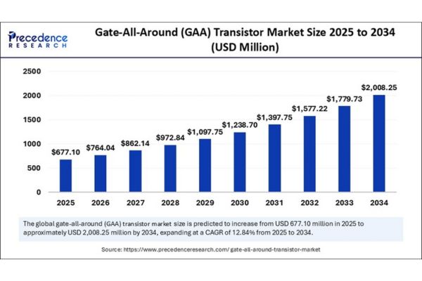
According to Precedence Research, the global Gate-All-Around (GAA) transistor market, valued at USD 677.10 million in 2025, is projected to surge to approximately USD 2,008.25 million by 2034, expanding at a robust CAGR of 12.84% from 2025 to 2034.
Innovations in transistor architecture, emerging from the void left by the limitations of FinFET technology, are powering a new generation of high-performance chips critical to AI, 5G, automotive, and next-generation electronics. With scalability and energy efficiency as the rallying cry, industry titans and nimble startups alike are racing to secure their futures in this pivotal market.
Gate-All-Around (GAA) Transistor Market Key Points
- The GAA transistor market is forecast to reach USD 2,008.25 million by 2034, up from USD 677.10 million in 2025.
- Asia Pacific leads with a 60% market share, driven by its strong foundry ecosystem, while North America is the fastest-growing region.
- Nanosheet GAA transistors command 55% of device architecture share, with rapid inroads from nanowire designs.
- High-performance computing (HPC) and automotive applications, including EV and ADAS chips, are market strongholds, each securing around 35% market share.
- Top industry players include TSMC, Samsung, Intel, and major design houses fueling fab innovation.
- The dominant end users are foundries (50% share), while Integrated Device Manufacturers (IDMs) are the fastest-rising segment.
- The research and growth wave in 3nm/2nm nodes foretell ongoing scale and breakthroughs from 2025 onward.
Revenue Table: By Region
| Region | Market Value 2024 (USD Mn) | Market Value 2034 (USD Mn) | CAGR (%) |
| Asia Pacific | 360.03 | 1,214.99 | 12.93 |
| Global | 600.05 | 2,008.25 | 12.84 |
The Role of Artificial Intelligence
Artificial intelligence is both a catalyst and a beneficiary of GAA transistor market growth. The demand for data processing, generative AI, and edge intelligence means AI models need chips that offer high throughput and minimal power leakage—areas where GAA technology excels. Chip designers are specifically optimizing GAA for AI-intensive workloads such as large language models, autonomous navigation, and image recognition, thus cementing the technology’s future relevance.
Beyond performance, AI is transforming how GAA transistors themselves are designed and manufactured. AI-enriched simulation, layout, and defect detection accelerate the development cycle while improving yields, enabling foundries to consistently deliver advanced chips at volume. This symbiotic relationship redefines the pace and scope of innovation, ushering in faster market deployments and more reliable fabrication.
What Is Driving the GAA Market Boom?
The insatiable need for performance and scalability at technology nodes below 3nm is pushing the industry beyond FinFET, rewarding the transition to GAA architectures. The architecture’s superior electrostatic control directly translates to enhanced efficiency and reduced energy consumption in smartphones, data centers, and EVs.
Industry-wide, breakthroughs in nanosheet and nanowire designs are enabling more compact, robust chips, fueling next-gen electronics and smart mobility.
What Opportunities and Trends Are Taking Center Stage?
Why Are Nanosheet GAA Transistors Gaining the Most Traction?
Nanosheet GAA transistors dominate with a 55% market share, offering exceptional drive current and manufacturability without the fiscal risks of reinventing foundry infrastructure. Their flexibility allows chipmakers to rapidly tune devices for server, mobile, and AI environments.
What Sets Nanowire GAA Designs Apart?
Nanowire designs are the fastest-growing segment (30% share), virtually eliminating leakage and empowering miniaturization at sub-3nm nodes key for AI accelerators and exascale computing.
Why Are 5nm/4nm Nodes Still King?
With early mass adoption, these nodes represent 45% of the market, underpinned by system-on-chip applications balancing innovation and affordability.
What’s Fueling Automotive and HPC Demand?
HPC leads applications (35%), driven by cloud, simulation, and AI training needs; the automotive sector likewise surges forward, as electric and autonomous vehicles require unprecedented chip sophistication.
Regional Analysis
Asia Pacific is the undisputed leader, accounting for 60% of the GAA transistor market thanks to powerhouse foundries, government initiatives, and a robust consumer electronics base. Prime contributors are Taiwan, South Korea, and China, who boast the world’s largest semiconductor fabricators and supply networks.
North America is the fastest-growing market, buoyed by innovation-heavy fabless companies, surging AI and cloud demand, and government programs supporting domestic manufacturing. Federal incentives and new fabs are rapidly closing the gap with Asia.
Segmentation Insights
Device Type/Architecture
Nanosheet GAA Transistors (55% share): Nanosheet GAA transistors dominate the market because their stacked sheet structure provides high drive currents and optimal electrostatic control. These devices are easier to integrate into existing manufacturing processes, making them preferred by foundries for scaling below the FinFET limits. Leading companies—including Samsung and TSMC—have commercial pilot production underway, which accelerates mainstream adoption for mobile, data-intensive, and AI-driven applications.
Nanowire GAA Transistors (30% share, fastest growing): Nanowire GAA transistors are growing rapidly due to their geometry, which completely encircles the channel and virtually eliminates leakage issues. They enable outstanding miniaturization at sub-3nm nodes and are uniquely valuable for high-performance computing and advanced AI chips, where energy efficiency and precision are critical. Research institutions and major fabs are prioritizing nanowire innovations, positioning them for future market growth.
Technology Node
5nm/4nm Nodes (45% dominant): Early adoption and commercial viability place 5nm and 4nm nodes at the forefront of the GAA market, backed by flagship products from leading foundries like Samsung. These nodes offer an optimal mix of innovation and manufacturability, supporting system-on-chip architectures for smartphones, servers, and laptops. Fabless semiconductor firms have further anchored their dominance by optimizing designs for these processes.
3nm/2nm Nodes (40% fastest-growing): The 3nm and 2nm nodes are projected as the fastest-growing segment because they offer unprecedented transistor density and energy efficiency. Their adoption is crucial for next-generation AI, HPC, and mobile applications. Though not yet mass-market, they represent the evolutionary leap to further miniaturization in response to Moore’s Law’s challenges.
Application
High-Performance Computing (HPC) (35% leader): HPC applications form the largest segment, driven by the insatiable demand for faster AI training, simulations, and analytics. Nanosheet GAA technology enables higher transistor density and precise electrostatic control, which data centers, cloud providers, and server manufacturers demand for efficiency and scalability. This segment assures consistent volume requirements, making it a primary driver for GAA adoption.
Automotive/EV (35% fastest-growing): The automotive sector especially electric vehicles and ADAS systems is the fastest-growing segment for GAA transistors. These chips power infotainment, navigation, and autonomous algorithms that require durable, efficient, and high-performance designs. The shift to smarter, greener mobility, supported by both government mandates and industry trends, is further amplifying the demand for advanced semiconductor solutions in vehicles.
End Users
Foundries (50% dominant): Foundries like TSMC, Samsung, and Intel command half the market by spearheading GAA mass production and innovation. Their scale helps absorb high upfront costs and complex yield optimization needs, making them central to the ecosystem. Close collaborations with design houses and government incentives reinforce their market position as technology enablers and gatekeepers.
IDMs (fastest-growing): Integrated Device Manufacturers (IDMs) are rapidly growing as they embed GAA architectures directly into proprietary products. This approach gives them tighter control over design and fabrication, and the capacity to deliver tailored, differentiated solutions for mobile, automotive, and AI-centric segments. The trend toward integrated innovation is accelerating GAA adoption among IDMs, making them the most dynamic end-user group in the segment.
Gate-All-Around (GAA) Transistor Market Companies
- TSMC
- Samsung Electronics
- Intel
- GlobalFoundries
- IBM Research
- ASML
- Applied Materials
- Lam Research
- KLA Corporation
- NVIDIA
- AMD
- Qualcomm
- Broadcom MediaTek
- Intel Foundry Services (IFS)
- SK hynix
- Micron Technology
- Cadence Design Systems
- Synopsys
- Arm Holdings
Challenges and Cost Pressures
Despite explosive growth, GAA faces hurdles: steep manufacturing complexity, high infrastructure investment needs, and persistent yield optimization issues. These factors make technology transitions demanding, especially for smaller foundries and cost-sensitive applications. Integration into legacy fabs also poses significant strategic and capital risks, slowing mainstream adoption outside major players.
Case Study: Samsung Electronics Co., Ltd. – Scaling 3nm GAA (MBCFET) Technology in 2025
Introduction
In the highly competitive semiconductor landscape, Samsung Electronics has consistently positioned itself as one of the pioneers in advanced chip manufacturing. The year 2025 marked a defining moment for the company as it successfully scaled and commercialized its second-generation 3nm Gate-All-Around (GAA) technology, branded as Multi-Bridge Channel FET (MBCFET™). This transition was not just an incremental step from FinFET to GAA but a major architectural leap that positioned Samsung ahead of competitors in both mobile and high-performance computing (HPC) segments.
This case study explores how Samsung leveraged its MBCFET™ innovation, forged strategic partnerships, and achieved tangible financial and technological gains.
Company Overview
- Company Name: Samsung Electronics Co., Ltd.
- Headquarters: Suwon, South Korea
- Core Business Units: Semiconductor Foundry, Memory, Consumer Electronics, Display, Mobile
- Foundry Competitiveness: Second largest global foundry player after TSMC, with a strong focus on cutting-edge nodes (3nm, 2nm, and beyond).
Offering – Samsung’s 3nm GAA-Based Process (MBCFET)
Samsung’s MBCFET™ represents a revolutionary transistor structure that overcomes the physical and performance limitations of FinFETs, which have been the backbone of chip manufacturing since 2011. Unlike FinFETs, which rely on 3D fins to control current, GAA uses nanosheets with gates wrapped around all four sides of the channel. This structure allows better electrostatic control, improved energy efficiency, and scaling potential for nodes below 3nm.
The key differentiation of Samsung’s approach is the Multi-Bridge Channel FET concept, where multiple nanosheets are stacked to provide design flexibility. This makes it easier for customers to balance performance and power requirements across a wide range of applications.
Detailed Case Study
In 2025, Samsung achieved a critical milestone: scaling its second-generation 3nm GAA technology for both smartphone system-on-chips (SoCs) and high-performance computing (HPC) processors.
1. Strategic Partnerships
- Qualcomm Collaboration: Qualcomm, one of the largest fabless semiconductor companies, partnered with Samsung to design AI-optimized 3nm SoCs for flagship smartphones. These chips integrated next-gen AI engines capable of real-time natural language processing and advanced image recognition.
- Nvidia Collaboration: Samsung’s 3nm MBCFET was also adopted by Nvidia for select HPC accelerators, particularly in AI data centers. The architecture provided efficiency gains needed to power large-scale AI training and inference workloads.
These partnerships were crucial in validating Samsung’s technology and expanding its footprint in markets traditionally dominated by TSMC.
2. Technical Achievements
Samsung’s 3nm GAA (second-gen) demonstrated significant advantages over its own 5nm and 4nm FinFET technologies:
- 20% performance improvement – critical for meeting the rising demand for AI processing in smartphones and HPC.
- 45% power reduction – extended battery life for mobile devices and reduced energy costs in data centers.
- High transistor density – allowed more powerful chips without increasing die size, essential for cost competitiveness.
3. Manufacturing Success
Scaling advanced nodes is a challenge that has delayed many chipmakers in the past. Samsung’s success in 2025 stemmed from:
- Heavy investment in EUV (Extreme Ultraviolet) lithography for nanosheet patterning.
- Proprietary process control algorithms ensuring yield improvement and defect minimization.
- A global network of fabs in Korea and Texas, supporting large-scale production.
Outcome
Samsung’s move to GAA yielded tangible results:
- 20% performance improvement for AI workloads and gaming in mobile SoCs.
- 45% power savings in HPC accelerators, helping reduce total cost of ownership (TCO) for data centers.
- Strengthened relationships with leading fabless players like Qualcomm and Nvidia, paving the way for future collaborations on 2nm nodes.
By delivering these improvements, Samsung proved its ability to mass-produce next-generation transistors at scale, an area where only a handful of players can compete.
Protectional – Intellectual Property Edge
One of Samsung’s biggest strengths in this case is its robust IP portfolio around MBCFET. Unlike traditional FinFETs, GAA introduces unique challenges around nanosheet stacking, gate-all-around integration, and yield optimization. Samsung’s patents cover:
- Nanosheet width modulation for custom power-performance trade-offs.
- Multi-bridge stacking techniques for higher drive current.
- Advanced EUV patterning to minimize variability.
This defensive IP strategy prevented replication by smaller competitors and secured Samsung’s long-term position in the GAA race.
Impact on the Market
The successful ramp-up of 3nm MBCFET™ technology had a ripple effect across the semiconductor industry:
- Smartphone Market: Flagship Android smartphones powered by Qualcomm’s 3nm SoCs showcased longer battery life, faster AI-driven features, and superior gaming performance. This raised consumer expectations and forced rivals to adopt GAA sooner.
- Data Centers: Nvidia’s adoption of Samsung’s GAA process improved energy efficiency in AI accelerators, reducing carbon footprints and aligning with sustainability goals.
- Competitive Landscape: Samsung became the first foundry to achieve high-volume production of GAA transistors, momentarily outpacing TSMC’s N2 ramp-up (scheduled for late 2025). This reinforced Samsung’s position as a technology leader rather than just a fast follower.
- Industry Adoption: By proving the viability of nanosheet GAA in commercial products, Samsung accelerated the broader industry shift away from FinFETs.
Financial After Implementation
The commercial success of Samsung’s 3nm GAA technology translated into significant financial gains:
- Within the first year of ramp-up, Samsung reported a USD 1.2 billion boost in its foundry revenue.
- This growth came largely from pre-orders by Qualcomm and Nvidia, both eager to integrate next-gen SoCs and HPC accelerators into their product lines.
- The new revenue stream strengthened Samsung Foundry’s contribution to the company’s overall semiconductor division, which also includes its dominant memory business.
- Long-term, the successful adoption of GAA positioned Samsung to capture greater market share in the global foundry business, which was valued at over USD 120 billion in 2025.
Lessons Learned
This case study highlights several broader lessons about the semiconductor industry and the transition to GAA:
- Early Innovation Matters: By investing in GAA early, Samsung positioned itself ahead of the curve.
- Partnerships Drive Validation: Collaborations with Qualcomm and Nvidia provided credibility and accelerated adoption.
- IP Protection is Critical: In an industry with trillion-dollar implications, patents and proprietary designs are as valuable as the technology itself.
- Sustainability is a Selling Point: Beyond performance, GAA’s energy efficiency addressed sustainability targets — a key purchasing factor for data centers.
Conclusion
Samsung Electronics’ successful scaling of 3nm GAA (MBCFET™) technology in 2025 represents a landmark achievement in the semiconductor industry. By combining technological breakthroughs, strong partnerships, robust IP protection, and market-focused execution, Samsung not only delivered superior performance and efficiency but also established itself as a true leader in advanced foundry services.
The financial uplift of USD 1.2 billion in revenue within the first year is only the beginning of what promises to be a long-term advantage in the era of nanosheet GAA transistors. More importantly, Samsung’s innovation catalyzed an industry-wide transition, setting new benchmarks for mobile devices, HPC, and beyond.


