
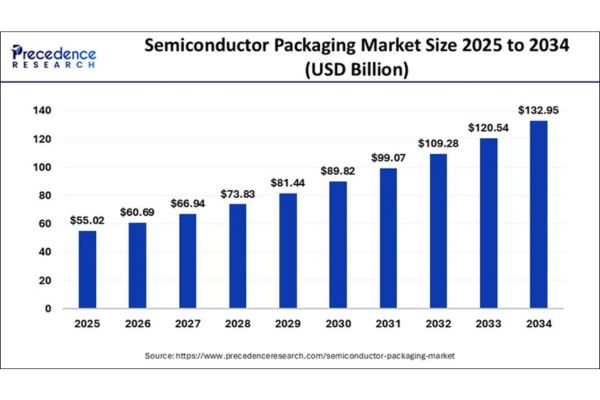
According to Precedence Research, the global semiconductor packaging market is projected to grow from USD 49.88 billion in 2024 to an impressive USD 132.95 billion by 2034, achieving a CAGR of 10.30% between 2025 and 2034.
This robust trajectory is fueled by rising adoption of high-tech consumer electronics, breakthroughs in communications infrastructure, and the relentless miniaturization of device architecture. Industry leaders and regional clusters especially in Asia Pacific are setting new benchmarks for technology and scalability.
Semiconductor Packaging Market Key Points
- The market will surpass USD 132.95 billion by 2034, up from USD 55.02 billion in 2025.
- Asia Pacific is the largest and fastest-growing region, accounting for USD 23.94 billion in 2024 and forecast to hit USD 64.84 billion by 2034 at a CAGR of 10.42%.
- Leading companies: TSMC, Samsung, SK Hynix are at the forefront of packaging innovation.
- The top technology segments: Flip-chip packaging dominates; Fan-Out Wafer Level Packaging (FOWLP) is the fastest-growing.
- Most in-demand end-user: Consumer electronics remains the largest application category.
Global & Regional Market Breakdown
| Category | Market Size 2024 | Market Size 2025 | Market Size 2034 | CAGR 2025-2034 |
| Global | USD 49.88 Billion | USD 55.02 Billion | USD 132.95 Billion | 10.30% |
| Asia Pacific | USD 23.94 Billion | USD 26.41 Billion | USD 64.84 Billion | 10.42% |
How Is AI Transforming Semiconductor Packaging?
AI is reshaping the semiconductor packaging industry across the value chain. In manufacturing, AI-enabled predictive analytics optimize yield rates, minimize material waste, and accelerate identification of production faults—driving efficiency and quality to new heights. In design, AI algorithms rapidly evaluate thousands of architecture permutations to find optimal thermal management and minimize electromagnetic interference, making next-generation packaging smarter and more reliable.
With the rise of edge computing and IoT devices, AI-powered tools are also enhancing the scalability of advanced techniques like Flip-chip and FOWLP by automating design adaptations and enabling smart diagnostics for mission-critical applications—from automotive ADAS to 5G network hardware.
What Are the Key Drivers for Market Growth?
Consumer electronics expansion: Widespread adoption of smartphones, wearables, smart TVs, and laptops is spurring demand for compact, efficient packaging solutions.
5G rollout: Upgraded networks require specialized RF and mm-Wave components, increasing the need for innovative packaging among telecom and communications players.
Automotive adoption: Growing integration of semiconductors in vehicles (ADAS, entertainment, powertrain, electric vehicles) means higher demand for durable packaging technologies.
IoT and cloud computing: Ever-smaller, low-power chips are essential for connected devices and high-performance data centers, boosting opportunities for advanced packaging.
How Do Industry Trends Shape Opportunities?
What new breakthroughs fuel packaging innovation?
Advanced techniques like System-in-Package (SiP), Fan-Out Wafer-Level Packaging (FOWLP), and 3D ICs are enabling more integration for smaller, lighter devices while improving power efficiency. Flip-chip packaging is rapidly overtaking traditional wire bonding by offering better heat dissipation, improved reliability, and higher connection density for high-frequency applications.
How are regions beyond Asia Pacific creating new opportunities?
Latin America’s emergence, propelled by rising demand and government tax incentives (notably in Brazil), is attracting more international manufacturers. Meanwhile, the Middle East and Africa are leveraging investments in smart cities and digital economies, especially in the UAE and Saudi Arabia—to expand advanced packaging adoption.
What makes organic substrates an industry favorite?
Organic substrates, primarily made from fiberglass-reinforced epoxy, combine low cost, satisfactory electrical performance, and high design versatility—creating fresh possibilities for applications in consumer electronics and communications.
Regional and Segmentation Analysis: The Press Perspective
Asia Pacific leads both in sheer volume and strategic innovation, boasting cutting-edge campuses like Taiwan’s Hsinchu Science Park. Massive investments in technology and talent make the region a global supply chain backbone. North America excels in R&D, nurturing ecosystems where chip designers, equipment makers, and startups collaborate to push packaging science forward.
Latin America and the Middle East & Africa are moving from emerging to influential, with Brazil pioneering incentives for technology parks and the UAE/Saudi Arabia investing in smart infrastructure.
Segmentation breakdown
By Type: Flip-chip, Fan-Out Wafer Level Packaging, Grid Array, Wire Bonding, and 3D ICs
By Packaging Material: Organic substrates, ceramics, metals, polymers
By Technology: System-in-Package, Fan-Out, Through-Silicon Vias, microchannels
By End-User: Consumer electronics (dominant), communications/telecoms (fastest growing), automotive electronics, industrial, IoT
What Are the Latest Breakthroughs and Who are the Top Players?
- TSMC – leadership in advanced IC packaging and 3D integration
- Samsung – breakthroughs in chip stacking and organic substrate engineering
- SK Hynix – fast-evolving packaging for memory chips and high-speed components
What Challenges and Cost Pressures Affect Market Players?
Manufacturers face mounting pressures to control costs amid intense competition. Reliability issues such as material fatigue, thermal stress, and failure risks in solder and wire bonds require ongoing refinement in both materials and engineering.
Managing heat dissipation has become critical as chips operate at ever-higher power densities. Global supply chain disruptions and raw material price volatility further challenge device makers to ensure uninterrupted operations.
Case Study: Material Needs and Measurement Challenges in Advanced Semiconductor Packaging
Background
The semiconductor industry has rapidly shifted from traditional packaging methods (like wire bonding and flip-chip) to advanced forms such as 2.5D/3D integration, fan-out wafer-level packaging, and heterogeneous integration. While much attention is given to silicon, interposers, and interconnects, the “soft side” of packaging — polymer-based materials like underfills, die attach adhesives, encapsulants, mold compounds, and thermal interface materials — plays an equally critical role.
These materials dictate mechanical stability, thermal performance, and reliability of the package. However, their behavior is far harder to predict and standardize than hard materials (like silicon or copper).
The Initiative
In 2025, a consortium of NIST (National Institute of Standards and Technology), NC State University, NREL (National Renewable Energy Laboratory), Intel, and other partners launched a joint initiative to map out the critical material and measurement challenges in packaging polymers.
The study “Material Needs and Measurement Challenges for Advanced Semiconductor Packaging: Understanding the Soft Side of Science” sought to answer:
- Why are polymer materials so hard to qualify for packaging?
- What measurement techniques and standards are missing?
- How can industry and research align to accelerate innovation?
Key Challenges Identified
- Long Material Adoption Cycles
- Unlike silicon innovations that may commercialize in 5–7 years, polymer materials often take 10–25 years to move from lab to high-volume production.
- This is due to stringent reliability requirements, lack of predictive models, and inconsistent performance across suppliers.
- Lack of Standardized Reference Materials
- The industry has no common “yardstick” for characterizing soft materials.
- For example, two labs may measure cure shrinkage or glass transition temperature of an underfill differently, leading to poor reproducibility.
- Measurement Gaps
- Critical properties such as residual stress, cure kinetics, warpage, and adhesion strength at interfaces are poorly measured with current tools.
- Advanced packaging creates multi-scale stress environments (from nanoscale bumps to large organic substrates) that polymers must withstand, but testing is not standardized.
- Process–Structure–Property Disconnect
- The behavior of packaging polymers is highly dependent on processingconditions (curing, pressure, temperature cycles).
- Today, there is a weak link between how materials are formulated, how they are processed, and how they ultimately perform in the package.
- Data & Modeling Limitations
- Multiphysics modeling of packaging reliability (thermal, mechanical, electrical) often relies on oversimplified polymer data.
- Without accurate inputs, simulations can’t fully capture delamination risks, void formation, or fatigue failures.
Industry Impact
- Reliability Risks: With AI accelerators, HPC chips, and EV power modules generating higher heat, weak links in polymer packaging can cause catastrophic field failures.
- Innovation Bottleneck: The slow adoption cycle means new packaging architectures (chiplets, fan-outs, glass interposers) are delayed by limitations in “soft” materials.
- Economic Costs: Failures traced to packaging polymers can cost millions in recalls or warranty claims.
Proposed Solutions & Recommendations
- Cross-Industry Consortia
- Establish partnerships (similar to SEMATECH for silicon) dedicated to packaging polymers.
- Jointly fund shared reference materials and testing protocols.
- Metrology Development
- Develop new measurement methods for:
- Residual stress at micro/nano scale
- Real-time monitoring of curing and adhesion
- Long-term degradation under cyclic thermal/mechanical loading
- Develop new measurement methods for:
- Standardization Efforts
- NIST and partners advocate creating standard reference materials for polymer testing, enabling labs worldwide to compare results consistently.
- Materials Informatics
- Use AI/ML + big materials datasets to predict how formulation changes affect properties and reliability.
- This shortens the 10–25-year cycle for new materials to reach industry.
- Closer Academia–Industry Collaboration
- Encourage “precompetitive research” where companies like Intel, TSMC, Amkor, and OSATs share data with universities to accelerate breakthroughs.
Takeaways
- This case study underlines that semiconductor packaging innovation is not only about silicon or copper — polymers matter just as much.
- Without better measurement science, standardization, and predictive modeling, the industry risks bottlenecks that slow the deployment of chiplets, AI chips, EV power modules, and photonics.
- The NIST-led initiative is a step toward creating a materials measurement ecosystem where advanced packaging can scale reliably, sustainably, and faster.


