

The Digital Twin in Semiconductor Market is moving from a specialized simulation capability toward a strategic technology layer for semiconductor design, manufacturing, packaging, testing, and lifecycle management. As chip architectures become more complex and fabs operate with increasingly sophisticated equipment and data flows, manufacturers are looking for ways to simulate production conditions, anticipate equipment failures, improve yield, and make manufacturing decisions before committing changes to the physical environment.
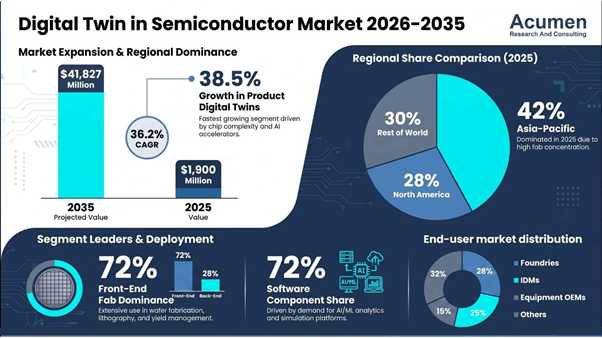
According to Acumen Research and Consulting, the Global Digital Twin in Semiconductor Market was valued at USD 1.90 billion in 2025 and is projected to reach USD 41.83 billion by 2035, representing a remarkable 36.2% CAGR between 2026 and 2035. The scale of this projected expansion reflects a broader shift from static engineering simulation toward connected, real-time and AI-enabled digital representations of semiconductor products, equipment, processes and fabs.
What Is a Digital Twin in Semiconductor Manufacturing?
A semiconductor digital twin is a virtual representation of a physical semiconductor product, piece of manufacturing equipment, process, production line, fab, or supply-chain operation. Unlike a conventional simulation, a digital twin can continuously incorporate real-world data from sensors, manufacturing execution systems, metrology equipment, process-control systems and other operational sources.
The objective is not simply to visualize a factory digitally. The more valuable proposition is the ability to simulate, predict, optimize and continuously learn from the physical semiconductor environment.
In practice, semiconductor digital twins can support:
- Process and recipe optimization
- Wafer-yield improvement
- Equipment health monitoring
- Predictive maintenance
- Defect detection and root-cause analysis
- Virtual commissioning
- Fab capacity planning
- Production scheduling
- Factory-layout optimization
- Advanced packaging and reliability analysis
This makes digital twin technology particularly relevant as semiconductor manufacturers move toward advanced nodes, heterogeneous integration, chiplets, high-bandwidth memory and AI accelerators.
Why Is the Digital Twin in Semiconductor Market Growing So Quickly?
The most important growth driver is the convergence of artificial intelligence, semiconductor manufacturing complexity and smart-factory investment.
Modern fabs generate enormous quantities of equipment, sensor, process, inspection and metrology data. Historically, much of this information has been used for monitoring and retrospective analysis. Digital twins create an opportunity to connect these datasets with physics-based models, AI, machine learning and simulation so that manufacturers can move from reactive decision-making toward predictive and eventually autonomous operations.
Acumen Research and Consulting identifies rising demand for AI-driven semiconductor manufacturing as a central market driver. Digital twins can combine real-time operational data with AI/ML models to predict yield, identify equipment problems and evaluate production strategies before changes are implemented on the factory floor.
The economics are becoming more compelling as semiconductor manufacturing capacity expands. Acumen estimates that global semiconductor manufacturing capacity could reach 11.1 million 300 mm wafers per month by 2028, compared with 10 million wafers per month in 2024. At the same time, advanced-node capacity of 7 nm and below is expected to reach approximately 1.4 million wafers per month by 2028, creating additional demand for sophisticated digital process modeling.
AI Is Turning Digital Twins Into Predictive Manufacturing Systems
The next phase of the Digital Twin in Semiconductor Market will be defined by AI.
Traditional digital twins primarily replicate physical systems and provide simulation capabilities. AI-enhanced twins can identify patterns across massive datasets, estimate future equipment behavior, recognize anomalies and recommend operational changes.
This distinction matters in semiconductor manufacturing because small variations in temperature, pressure, deposition, etching, lithography or other process conditions can have downstream effects on wafer yield.
AI-powered digital twins can therefore become a decision-support layer between physical manufacturing equipment and fab-management systems. Instead of simply reporting that equipment performance has changed, an intelligent twin can potentially estimate why the change occurred, determine how it could affect production and evaluate corrective actions digitally.
The emerging combination of physics-informed AI, machine learning, accelerated computing and real-time factory data is consequently one of the most important technology trends shaping semiconductor digital twins.
Process Digital Twins Currently Lead the Market
Among digital twin types, process digital twins accounted for 48% of the global market in 2025, according to Acumen Research and Consulting. Their leading position reflects the importance of process optimization, yield improvement, defect reduction, virtual experimentation and real-time process control in semiconductor manufacturing.
Semiconductor fabrication involves hundreds of tightly controlled processing steps. Digital process twins allow manufacturers to model variables before performing physical experiments, potentially reducing costly trial-and-error cycles.
However, the market is gradually moving beyond process-level applications.
Acumen projects the product digital twin segment to be the fastest-growing digital twin type, with a 38.5% CAGR through 2035. Product twins connect semiconductor product characteristics with design, manufacturing, performance, reliability and lifecycle information. Increasing chip complexity, advanced packaging, heterogeneous integration and AI accelerators are strengthening this use case.
Software Dominates, but Services Are Becoming More Important
Software represented 72% of the Digital Twin in Semiconductor Market in 2025, making it the dominant component category. Semiconductor digital twins require simulation platforms, modeling engines, AI/ML algorithms, data-management systems, analytics and industrial connectivity.
Yet services are expected to grow even faster. Acumen forecasts a 38.2% CAGR for services from 2026 to 2035, reflecting the complexity of implementing digital twins in semiconductor environments. Services include system integration, data engineering, model development, customization, implementation, cybersecurity, training, maintenance and ongoing optimization.
This suggests that future competition will not be limited to software functionality. Providers will increasingly compete on their ability to integrate heterogeneous manufacturing data and translate digital-twin models into measurable fab outcomes.
On-Premises Deployment Remains Important
Security and intellectual property considerations have a major influence on digital twin deployment.
Acumen reports that on-premises deployment accounted for 42% of market revenue in 2025, while cloud deployment held a 34% share and hybrid deployment accounted for 24%.
For semiconductor manufacturers, the appeal of on-premises environments is straightforward. Advanced-node process information, equipment data, manufacturing recipes, product designs and intellectual property are among the industry’s most sensitive assets.
At the same time, cloud infrastructure provides access to scalable computing, storage and AI capabilities. The likely long-term direction is therefore not simply “cloud versus on-premises,” but increasingly sophisticated cloud-edge-fab architectures capable of balancing computational requirements with security and latency.
Front-End Manufacturing Represents the Largest Opportunity
The front-end segment accounted for 72% of the market in 2025, according to Acumen. Front-end fabrication involves processes such as lithography, deposition, etching, ion implantation, cleaning, chemical mechanical planarization, metrology and inspection.
These operations generate substantial volumes of highly granular data and require extremely precise control.
However, back-end semiconductor manufacturing is becoming increasingly attractive as advanced packaging grows in importance. Acumen estimates that the back-end segment represented 23% of the market in 2025. Digital twins can support package design, thermal modeling, mechanical-stress analysis, assembly optimization, testing and reliability prediction.
The rise of chiplets, 2.5D and 3D integration, high-bandwidth memory and heterogeneous architectures should therefore broaden digital twin applications across the semiconductor value chain.
Which Companies Are Major Players in the Digital Twin in Semiconductor Market?
The ecosystem is unusually broad because no single category of technology provider controls every layer of a semiconductor digital twin.
According to Acumen Research and Consulting, key companies include NVIDIA Corporation, Siemens AG, Synopsys, Inc., Ansys, Inc., Cadence Design Systems, Inc., Dassault Systèmes SE, PTC Inc., Schneider Electric SE, Rockwell Automation, Inc., Autodesk, Inc., IBM Corporation, Microsoft Corporation, Applied Materials, Inc., and Lam Research Corporation.
Their competitive positions differ considerably.
NVIDIA is particularly influential in accelerated computing, AI infrastructure and physically accurate simulation environments. Its Omniverse platform is being used in semiconductor-factory digital-twin initiatives.
Siemens brings industrial automation, manufacturing software and digital-twin capabilities together through its broader industrial technology ecosystem.
Synopsys, Ansys and Cadence have strong positions around semiconductor design, electronic design automation, physics-based simulation and engineering workflows.
Applied Materials and Lam Research have a different strategic advantage: deep knowledge of semiconductor manufacturing equipment and processes. Applied Materials, for example, describes its AppliedTwin framework as a solution for virtualizing semiconductor processes and equipment using sensor and metrology data.
This ecosystem means that the Digital Twin in Semiconductor Market is best viewed as a technology convergence market, rather than a conventional software category.
Which Countries Have the Highest Concentration of Digital Twin Providers?
There is no single authoritative global ranking of digital-twin providers by country because the ecosystem spans EDA companies, industrial automation vendors, semiconductor equipment manufacturers, cloud providers, AI companies and specialist software developers.
However, the strongest provider concentration is clearly associated with major semiconductor technology hubs.
United States
The United States has one of the deepest concentrations of digital-twin technology providers. Major EDA, AI, cloud, industrial software and semiconductor-equipment companies are headquartered or have substantial operations there.
Acumen identifies the U.S. as the leading country within North America, where digital-twin adoption is being reinforced by domestic fab investment and intelligent-factory development.
Germany and Broader Europe
Germany is particularly important because of its industrial automation and engineering ecosystem. Siemens provides a major bridge between industrial digital twins, automation and semiconductor manufacturing.
Europe more broadly has strong positions in industrial software, simulation, automation and engineering technologies.
Taiwan
Taiwan is strategically important because of its exceptionally high concentration of advanced semiconductor manufacturing. This makes it not only a major adopter of digital twins but also an important development environment for fab-specific applications.
Japan and South Korea
Japan and South Korea combine sophisticated semiconductor manufacturing, electronics and industrial-automation ecosystems. Their smart-factory and semiconductor modernization initiatives provide fertile ground for digital-twin adoption.
China
China has a large and expanding semiconductor manufacturing base alongside major investments in industrial digitalization, AI and smart manufacturing. Its domestic semiconductor development is increasing the potential market for digital manufacturing technologies.
How Do Regional Digital Twin in Semiconductor Markets Compare?
Asia Pacific: The Global Leader
Asia Pacific dominated the Digital Twin in Semiconductor Market with a 42% share in 2025, according to Acumen. The regional market was approximately USD 798 million in 2025 and is projected to reach about USD 19.66 billion by 2035, representing a 37.9% CAGR.
The region’s advantage comes from its concentration of semiconductor fabs, equipment manufacturers, advanced-node production and manufacturing investment.
Taiwan is particularly significant because of its advanced foundry ecosystem, while China, South Korea and Japan contribute substantial semiconductor manufacturing and electronics capabilities.
North America: Design, AI and Advanced Manufacturing
North America held a 28% market share in 2025, making it the second-largest regional market. Acumen estimates the region will grow at a 34.5% CAGR from 2026 to 2035, reaching approximately USD 10.46 billion by 2035.
The region’s competitive advantage lies in its combination of semiconductor design, EDA, AI, cloud computing, semiconductor equipment and domestic fab investment.
Europe: Engineering and Industrial Automation
Europe’s opportunity is strongly connected to industrial automation, engineering simulation, sustainability and semiconductor sovereignty. Digital twins can help European manufacturers improve production efficiency while supporting the region’s broader push toward advanced semiconductor capabilities.
Emerging Markets
Latin America and the Middle East & Africa currently represent smaller portions of the market, but semiconductor ecosystem development, smart manufacturing and digital infrastructure investment could create longer-term opportunities.
What Are the Biggest Challenges Facing Semiconductor Digital Twins?
The technology’s growth is not without obstacles.
The first is data integration. Semiconductor fabs contain equipment from multiple generations and vendors, with different data formats, protocols and levels of data accessibility.
The second is model fidelity. A digital twin becomes valuable only when its representation of the physical system is sufficiently accurate for the intended decision.
Third is cybersecurity. Connecting production equipment, intellectual property and operational data creates additional attack surfaces.
Fourth is implementation complexity. A successful fab-level digital twin can require expertise across semiconductor process engineering, industrial automation, software architecture, AI, physics modeling, cybersecurity and data engineering.
These challenges explain why services are becoming such a rapidly growing component of the market.
The Next Stage: From Equipment Twins to Autonomous Fabs
The long-term opportunity is not simply to create more digital replicas. It is to connect them.
A future semiconductor factory could combine equipment twins, process twins, product twins, fab twins and supply-chain twins into a continuously connected digital environment.
Acumen’s technology roadmap points toward AI-enabled equipment twins, real-time process twins, multi-equipment production-line twins, fab-level twins, physics-informed AI, and cloud-edge digital-twin infrastructure over the coming decade.
This evolution could fundamentally change how semiconductor fabs are designed and operated.
Instead of commissioning a physical production line and optimizing it after startup, manufacturers could increasingly simulate layouts, equipment interactions, production schedules and capacity scenarios before making physical investments.
Instead of waiting for equipment failures, operators could predict them.
Instead of relying primarily on physical experimentation to optimize recipes, engineers could test scenarios against physics-based and AI-enhanced models.
And instead of treating manufacturing, design, testing and lifecycle management as separate processes, digital twins could connect them through a continuous digital thread.
Strategic Outlook for the Digital Twin in Semiconductor Market
The Digital Twin in Semiconductor Market is becoming strategically important because the semiconductor industry is simultaneously confronting rising chip complexity, expensive fab investments, tighter production tolerances, advanced packaging requirements and enormous data volumes.
The strongest opportunities will likely emerge where digital twins are combined with AI, machine learning, accelerated computing, industrial IoT, physics-based simulation, edge computing and semiconductor process expertise.
The Digital Twin in Semiconductormarket’s projected expansion from USD 1.90 billion in 2025 to USD 41.83 billion by 2035, at a 36.2% CAGR, underscores the scale of this transition, according to Acumen Research and Consulting.
The central question is therefore shifting from whether semiconductor manufacturers should use digital twins to where they can create the greatest operational value.
For leading-edge fabs, the answer increasingly lies in connecting the digital twin to the entire semiconductor lifecycle—from design and process development to equipment management, wafer fabrication, advanced packaging, testing, yield optimization and production planning.
That is where the next generation of semiconductor manufacturing intelligence is likely to emerge.