
A printed circuit board (PCB) may pass light-load bench tests with default autorouter settings, 10-mil traces and a single ground plane, but those choices can fail at industrial power levels. Higher current and switching stress can create hot spots, erratic control signals or transistor failures.
Optimizing PCB layout for high-power applications means controlling where current flows, where heat builds up and how noise returns through the board. Engineers must size copper paths, minimize switching loops, place decoupling capacitors carefully, manage grounding and set clearance and creepage distances according to voltage and operating conditions. Each decision affects the others, so reliability depends on treating the layout as one electrical, thermal and insulation system.
Sizing Conductors for High-Current PCB Design
Before selecting trace width and copper thickness, engineers should establish continuous current, allowable temperature rise and acceptable voltage drop.
For high-current PCB design, that assessment should include:
- Continuous current
- Allowable temperature rise
- Acceptable voltage drop
- Connector lands
- Pad exits
- Layer transitions
In a trace-sizing investigation that examined layer count, substrate material and copper thickness, trace-sizing tools accurately determined the current-carrying capability in the tested FR4 glass-epoxy boards. Prediction accuracy was highest for two-layer constructions, while ceramic and aluminum substrates exhibited temperature discrepancies. Calculated outputs therefore remain construction-dependent estimates.
Internal and external conductors need separate checks against the selected calculation method. The design record should identify the stackup, finished copper thickness and assumptions behind each width calculation. Where a route changes layers, engineers should compare via count and barrel plating with the fabricator’s specifications.
Prototype measurements can then test those assumptions under representative loading. Recording both conductor temperature and voltage drop provides the team with specific results to compare against its electrical and thermal acceptance criteria.
Minimizing Switching-Loop Area With Decoupling Capacitor Placement
During placement, engineers should identify the converter’s high-frequency current paths. From there, they can evaluate loop inductance, voltage overshoot and ringing against device limits. That assessment should include whether the switching loop is compact, whether the return path stays close to the outgoing current and whether the stackup supports low-inductance routing.
In the buck stage, engineers should place and route the input bypass capacitor so that the high-frequency current loop between the capacitor, the high-side supply and the low-side return stays as short as possible. The device’s recommended layout provides a reference for the compact commutation-loop arrangement, including any adjacent-layer routing and its associated return path.
Switch-node copper and sensitive control traces also need a coupling check. Component documentation should guide decoupling selection, including effective capacitance under bias, ripple-current ratings and expected temperature for the selected topology.
In industrial ultrasonic equipment, engineers should also account for losses in the driven transducer, as these can affect the system’s total heat load. Hard piezoelectric ceramics engineered to resist dielectric loss offer relatively low dielectric dissipation and lower susceptibility to heat-induced depolarization under high-duty-cycle conditions. Because these properties apply to the transducer rather than the PCB’s decoupling capacitors, engineers should evaluate them separately when tracing heat sources.
Managing PCB Thermal Loads Through Copper and Vias
For surface-mount power packages, PCB thermal management starts with the designated thermal connections and available copper area. Package guidance should also clarify which electrical connections to underlying planes are permitted, particularly where the thermal connection shares a power-device terminal.
A thermal-via investigation used computational fluid dynamics to examine the effects of diameter, spacing, plating thickness and conductive fill and then validated an optimized configuration through prototyping and testing. The results showed that these parameters work together rather than independently. Designers should therefore evaluate via geometry, plating and fill as a combined thermal strategy for the array.
Before finalizing a via array, engineers need to compare its geometry with fabrication capabilities and the package footprint. Assembly planning should address solder loss and the suitability of filled or capped vias. The selected construction belongs in the manufacturing documentation alongside the thermal pad requirements.
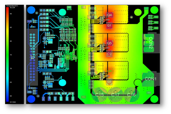
Enclosure testing should evaluate the assembled thermal design under sustained load. Acceptance criteria should cover both the power devices and nearby temperature-sensitive components, while the test record captures airflow and ambient conditions.
Designing Grounding Architecture to Keep Power Noise Out of Logic
Grounding decisions should start with a continuous reference plane, careful component placement and the device manufacturer’s layout instructions. Engineers also need to keep gate-drive returns and sensitive measurement connections away from noisy power-current paths whenever the topology allows.
A signal crossing a reference-plane split creates large loop inductance that can contribute to distortion and radiated emissions. In the investigated multilayer-board arrangement, carefully positioned stitching vias restored suitable return paths.
Before adding connections in real-world applications, engineers should confirm which reference regions share a schematic net and where designated isolation barriers must remain intact. Stitching vias may be helpful when reference regions are intended to share the same electrical net, but they should not bridge areas that are intentionally isolated. Connector transitions, board cutouts and signal-layer changes also warrant checks for reference continuity.
Checking Clearance, Creepage and Isolation for High-Voltage Safety
Clearance concerns the shortest through-air separation between conductors, while creepage follows the insulating surface. The applicable equipment standard specifies the requirements for each boundary, so the design record must identify the governing criteria.
Working voltage, expected transients, altitude and pollution degree belong in the spacing assessment. Where governing creepage rules require it, the material’s comparative tracking index must also be documented. Before release, engineers should check final dimensions against manufacturing tolerances, connector geometry and exposed hardware.
Testing of five fiberglass circuit-board electrode configurations found that electrode geometry and insulation spacing strongly influenced partial-discharge behavior and breakdown resilience. The study measured partial-discharge inception voltage and breakdown voltage across parallel, triangular, right-angled and floating-electrode designs, with results varying by configuration. Engineers should therefore treat clearance and creepage decisions as geometry-dependent design choices and validate insulation performance under the expected electrical stress.
Building Reliability Into Industrial Power Boards
Before production release, engineers should document how the layout meets current capacity, heat removal, grounding, switching noise and insulation requirements. Acceptance criteria should connect to calculations, component requirements or prototype results. Resolving any remaining design gaps before fabrication approval can help teams carry verified design assumptions into production. That discipline supports a more consistent transition from bench testing to industrial operation.
About the author
Jack Shaw is the senior editor of the men’s lifestyle magazine Modded and has written extensively about electric vehicles, sustainable practices and maintaining a green lifestyle through your everyday actions. His writing can be found in Green Living Journal, Packaging Digest, EcoHotels and more.