
The Forlinx Embedded T153 development board series is a lineup of products built around the Allwinner T153 industrial-grade processor. This series includes the FET153-S System on Module (SoM) and the OK153-S development board, both designed to offer industrial-level reliability and powerful multi-core heterogeneous computing. These boards are ideal for demanding applications across various industries like industrial automation, power management, and new energy sectors.
As an officially certified partner of Allwinner Technology, Forlinx Embedded is among the first manufacturers to introduce this SoM series to the market.
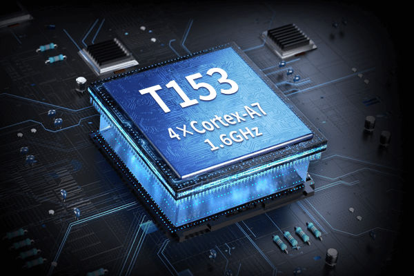
It is based on the Allwinner T153 processor, which is specifically designed for the industrial field. It integrates a 4-core Cortex-A7 (with a main frequency of 1.6GHz) and an independent RISC-V E907 core (with a main frequency of 600MHz), forming a multi-core heterogeneous architecture that can simultaneously meet the requirements of efficient data processing and real-time control. The SoM has passed strict industrial environment tests in Forlinx Embedded’s laboratory. It supports a wide temperature range of -40°C to +85°C for operation and has a lifespan of 10-15 years, ensuring long-term and stable product supply.
It uses the “edge connector + LGA” connection method to lead out all 185 pins of the CPU (the pin pitch of the stamp hole is 0.4mm, and that of the LGA package is 0.47mm). Users can flexibly configure the hardware according to the scenario. The supporting OK153-S development board further optimizes the interface layout and simplifies the secondary development process.
Specification Parameters
| FET153-S System on Module Basic Features | |
|---|---|
| CPU | Allwinner T153 |
| ARM: | 4×Cortex-A7,up to 1.6GHz |
| RISC-V | E907, up to 600MHz |
| NPU: | No |
| GPU: | G2D |
| VPU: | No |
| RAM | 256MB/512MB/1GB DDR3 |
| ROM | 256MB/512MB NandFlash /8GB eMMC |
| Operating Temperature | -40℃~+85℃ |
| Working Voltage | DC 5V |
| Connection | Edge connector + LGA, with a total of 185 pins led out. The center-to-center spacing of the edging connecting pins is 0.4 mm. The pitch for LGA package is 0.47 mm. |
| OS version | Linux5.10 |
| Flashing | USB OTG |
| Dimensions | 44mm x 35mm |
| FET153-S System on Module Functional Parameters | ||
|---|---|---|
| Function | Quantity | Parameter |
| Parallel CSI | ≤1 | Supports 8/10/12/16 bit wideth and BT.656 up to 2-ch 720P@30fps and BT.1120 up to 2-ch 1080P@30fps,RAW up to 4-ch720P@30fps |
| MIPICSI | ≤2 | Supports 4-lane/2+2-lane,Upto1.0Gbit/sperlane |
| MIPIDSI(1) | ≤1 | Supports 4-lane MIPI DSI, Up to 1920×1200@60fps,1.0Gbit/sperlane |
| RGBLCD(1) | ≤1 | DE/SYNC mode, up to 1920×1080@60fps;RGB888, RGB666 and RGB565 pixel |
| LVDS(1) | ≤2 | Up to 1920×1080@60fps for dual link; Up to 1366×768@60fps for single-link |
| SDIO | ≤2 | SMHC0 for SD card; SMHC1 for SDIO interface, 3.3 V mode only |
| Audio | ≤1 | Built-in audio codec supports 1 x differential LINEOUT output |
| IIS | ≤3 | Supports master/slave mode, sampling rate 8kHz to 384kHz; I2S0/2 supports 4lane application; I2S1 supports 2lane application |
| DMIC | ≤1 | Supports master/slave mode with sampling rate from 8kHz to 48kHz |
| OWAIN/OUT | ≤1 | Single line audio |
| USB2.0 DRD | 1 | Supports master and slave and High-Speed,480Mbps |
| USB2.0 HOST | 1 | Only supports master mode, and High-Speed, 480Mbps |
| GMAC | ≤3 | Supports RMII/RGMII interface and rate 10/100/1000 Mbit/s |
| CAN-FD | ≤2 | Supports CAN-FD(upto64databytes) and CAN2.0A CAN2.0B |
| LocalBus | ≤1 | Supports 8/16/32 bit width, up to 100MHz bus clock |
| SPI | ≤4 | Supports master/slave mode with up to 100MHz clock; SPI0, SPI2, SPI3 support SPI mode; SPI1 supports SPI mode and DBI mode |
| TWI | ≤5 | Compatible with I2C standard, standard mode 100kbit/s, fast mode 400kbit/s |
| UART(2) | ≤10 | Compatible with industry standard 16450/16550. |
| GPADC | ≤24 | 12-bit sampling resolution, maximum sampling rate 1MHz; GPADC2 has 4 channels multiplexed as TPADC |
| TPADC | ≤1 | 4-wire resistive touch, 12 bit SAR type AD conversion |
| PWM&PWMCS | ≤30 | PWM output frequency 0 ~ 24 MHz or 0 ~ 100MHz; PWMCS output frequency 0 ~ 4MHz, supporting maximum and minimum frequency limit |
| LEDC | ≤1 | Control LED light, programmable output high and low width, data up to 800kbit/s |
| IRTX | ≤1 | Infrared output |
| IRRX | ≤4 | Infrared receiving |
| GPIO | ≤140 | |
Note: The parameters in the table are hardware design or theoretical CPU values.
(1) MIPI-DSI have a pin multiplexing relationship, please read the chip data sheet or pin multiplexing table;
(2) UART0 is used as the debugging serial port. It is recommended to keep this design.
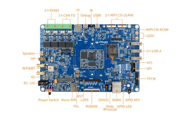
OK153-S Development Board:
The SoM comes with a supporting OK153-S development board. The SoM and the carrier board are connected using the edge connector + LGA leading out the functional pins of the processor in the most convenient way. In – depth optimization has been carried out for different functions, which facilitates users’ secondary development and simplifies the user design, providing a good basis for evaluation and design for your project.


