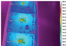


Power devices made of silicon carbide (SiC) are becoming more prominent in various applications that require high efficiency, compactness, and high temperatures of operation. SiC MOSFETs can switch at higher frequencies, thus creating much lower conduction losses and reaching junction temperatures around 175 degrees.
The advantages of the technology create tougher requirements for the packaging of the power modules. The packaging process should take into consideration electrical, thermal and mechanical designs as the packaging parasitics can affect the performance of the devices.
The Significance of Packaging for SiC Technology
Switching the material from silicon to SiC leads to a remarkable change in the design of semiconductor devices as it takes place in nanoseconds, thereby raising the importance of parasitic inductance and capacitance. Besides, the thermal cycling can reach over 1000 cycles, causing stress on the device’s parts.
Modern packaging makes it possible to minimize electrical distance, enhance heat dissipation as well as control thermal gradients.
Important Packaging Methods
In today’s times, different innovations have been introduced in order to handle the electric and thermal requirements. Direct-bonded copper (DBC) substrates have been around for some time now and they are still prevalent in usage owing to their capability to insulate while simultaneously minimizing thermally resistive paths. Thickness of copper used can vary from 0.3 mm to 0.8 mm based on the thermal and electrical requirements.
One more important technological method is silver sintering. Instead of the traditional technique of soldering, this method uses pressure assisted or pressureless sintering of silver in order to create thermally conductive thin connections. The thickness of connection can range from 20 to 100 micrometers providing the possibility of reduction in thermal resistance.
Heating Considerations and Dependability
SiC components can perform well at a high operating temperature, but higher operating temperature does not eliminate the importance of meticulous thermal design. The total thermal resistance of a device is determined by semiconductor chip, chip connection, substrate, mechanical base-plate, and cooling interface. A cumulative reduction in thermal resistance by 0.05 K/W contributes to a decrease in a junction temperature for high power levels.
Dependability is closely related to temperature variations. Each material has a different coefficient of temperature expansion thus repeated heating and cooling cycles may lead to solder joint, wire bond or substrate failures.
| Packaging Parameter | Typical Advanced Target | Main Benefit |
| Bond-line thickness | 20–100 µm | Lower thermal resistance |
| Stray inductance | Below 10 nH | Reduced voltage overshoot |
| Junction temperature | Up to 175°C | Higher operating capability |
| Copper layer thickness | 0.3–0.8 mm | Improved current and heat spreading |
High Switching Speed Electrical Design
The crucial factor in designing layouts for ICs arises not merely out of semiconductor technology but rather from the considerations underlying high-speed switching technology.
The layout must minimize the inductance of all terminals, decrease the length of current paths, and link power circuits closely between each other. The commutation-loop inductance reduction from 10 nH to 5 nH approximately halves the inductive voltage being created at the same current slew rate.
The connections between gates and drivers are to be regarded with great attention, too. For instance, by using the Kelvin-source principle, it is possible to separate the gate drive return path from the high current return way, thus decreasing the common source inductance. This seems to be most helpful, when switching silicon carbide devices where the current slew rate is equal to several hundreds of amps per microsecond.
Changes in Materials and Structures
Recent innovations in SiC packaging include the use of materials that are more suitable for high-temperature applications and multiple thermal cycles. Three materials – copper, aluminum nitride, and silicon nitride substrates – are designed differently in terms of thermal conductivity, mechanical properties, and manufacturing costs. For instance, silicon nitride substrates provide great fracture toughness when subjected to extreme thermal cycling.
Another innovation is the design of modules with no baseplate. By eliminating the usual baseplate, a smaller thermal interface and weight of the package are achieved, since direct cooling devices enable shorter thermal path. Additionally, in some designs, double-sided cooling positions the heat paths above and below the semiconductor, improving heat extraction efficiency and reducing thermal gradients.
Obstacles to Overcome
The global market for SiC Power Module Packaging was estimated at $2.8 billion in the year 2025, according to Data Intelo. The market is determined to expand to $7.4 billion by 2034, representing an 11.2% compound annual growth rate. This growth is taking place against the backdrop of increasing technical advancements in terms of lower parasitics, better thermal management, and increased reliability in high-power applications.
Nevertheless, advanced packaging continues to pose more issues because it remains non-standardized. Hence, there must be manufacturing tolerances, as well as established inspection methods for detecting faults like voids or delaminations.
Next-gen SiC modules will comprise low-inductance routing as well as high-temperature materials possessing improved thermal paths. The relevance of having packaging with temperature measurement, as well as current information and diagnostics, will be quite vast for servicing purposes.
In addition, with the increasing switching frequency that surpasses 100 kHz in certain applications, packaging will influence to a considerable degree the level of SiC utilization regarding its electric features.
Final Thoughts
The packaging of SiC power modules has gone beyond being just a protective covering to become an integral aspect of thermal and electrical engineering. Packaging now incorporates low-inductance interconnects, sintered layers of between 20 and 100 micrometers, substrates with comparatively high performance and technology for cooling to nearly 175 degrees Celsius.
Progress in future technologies will depend on how effectively efficiency, reliability, manufacturability, and cost can be balanced. Packaging will be crucial in development of SiC devices.
About Author
Ashish Kolte is a Marketing Manager at DataIntelo with expertise in marketing, market intelligence, and business strategy. He combines marketing insights with industry research to analyze market trends, identify growth opportunities, and provide data-driven perspectives on emerging industries and global business developments.