
Abstract
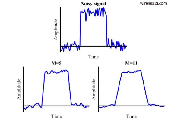
This article presents a finite impulse response (FIR) moving-average filter for validating noisy analog signals. While the conventional sliding-window implementation is computationally efficient, it requires storing the last N – 1 samples, leading to significant memory usage for large windows. To address this limitation, an alternative method is proposed that avoids full sample history storage by integrating the filter state with incoming samples. The approach is applied to a charger controller for validating the termination current of a lithium-ion battery, demonstrating reduced memory requirements and simplified implementation.
Introduction
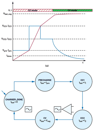
The charging process for a lithium-ion battery (Figure 1a) differs from that of a normal battery,1–6 depending on the battery’s state-of-charge (SoC); for example, the voltage and current values. More specifically, there are two different analog control loops (voltage loop and current loop) that are based on the charging region and act on the battery to regulate the voltage or the current. Initially, the current loop is the dominant one, so charging starts with constant current; the voltage rises steadily, and whenever it exceeds specific programmable thresholds, the value of the current changes accordingly. Once the maximum regulated voltage is reached, there is a change in the control loop; the voltage loop will become the dominant one, and charging continues with constant voltage while the current gradually decreases until the battery is fully charged. The parameter that determines which control loop is dominant is the GMV signal, which represents the effective transconductance (gm) of the voltage loop. In particular, GMV indicates the dominance of the voltage loop, whereas GMI indicates the dominance of the current loop. Since GMV results from the interaction between different analog control loops, it may exhibit instability and fluctuations, thus requiring filtering.
Moreover, during the constant voltage phase (CV), in which GMV is dominant, the charging current gradually decreases toward very small values, where noise, ripple, and electromagnetic interference (EMI) make it increasingly difficult to reliably identify the true termination point. These uncertainties can lead to premature termination or inaccurate end-of-charge (EoC) detection that could be resolved in different ways.7–11
This is where the filter comes into play, dynamically calculating and updating the average GMV and Idone signals within a given time interval by assuming that the whole architecture includes a processor that samples the battery voltage/current at a specific rate (usually around 100ms) and sends the results to the charger finite state machine (FSM) to make it evolve.
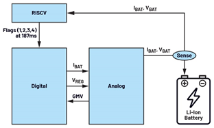
A simplified state diagram of a charger controller is shown in Figure 1b, where each transition is well defined by the voltage/ current threshold. Figure 2 shows the block diagram of the charger architecture and relates the signals to the arcs of Figure 1b. It appears that all the transitions are triggered by the RISCV processor (via flags monitoring battery voltage and current), except for the GMV analog signal that defines the constant-current to constant-voltage transition. The battery can be considered fully charged when the current goes below a precise value, indicated with Idone, typically equal to 150µA, and that is measured through a high-performance ADC whose resolution is limited by the K·T/Q noise. In the considered architecture, Flag4 (Idone measurement in Figure 1a) is updated at a specific rate, thus defining that the termination of the charger process must be correlated to the GMV signal. To declare the battery fully charged, there must be both the constant-voltage loop active and current below the Idone threshold. To do this, another filter was used, designed following the same filtering approach used for the GMV signal.
Proposed Filter Design
Traditionally, a common debounce circuit has been used to monitor the unstable GMV signal coming from the analog charging circuit. This could cause a long delay in the GMV validation, since every time the signal changes value (due to an unwanted glitch), the debounce circuit restarts the count.
The proposed approach consists of a moving average filter, which is a particular finite impulse response (FIR) filter12 whose output sequence is given by:

Where h[k] represents the filter impulse response and x[n-k] is the generic input sequence. In this design, all the coefficients of the impulse response have the same value equal to 1/N where N is the number of samples averaged; therefore, Equation 1 becomes:

This is a majority filter that calculates a moving average of the last N available samples using an observation window equal to N/2. The proposed approach requires a small number of memory elements (flip-flops) for a long observation period and does not need any circular buffer to memorize the samples. The simplified diagram of the proposed architecture is shown in Figure 3a, where an up/down counter, representing the filter, is incremented each time IN is high and decreased when IN is low. The filter sets IN_valid when the counter reaches its maximum value and resets the output when its count is zero. The first case occurs when there have been more ones than zeros in the last period; for example, the observation window has all the samples equal to 1 (since it contains N/2 samples). Conversely, IN_valid is cleared when there are more zeros than ones among the last N samples; for example, all the samples in the window are equal to 0. The counter value represents the number of ones/zeros within the semi-period; when this value increases, it means removing a 0 and adding a 1 inside the observation window (and vice versa), just like a moving average filter. So, based on the filter output, it is possible to determine if the average of the last N samples is greater (or lower) than 0.5. Note that each time a new sample arrives, the oldest one is removed from the observation window by increasing (decreasing) the counter, and the average is dynamically recalculated. If the window is full of ones (zeros) for the last semi-period, the signal can be assumed high (low). The latch in Figure 3a changes the output only when all zeros or all ones appear in the counter output.
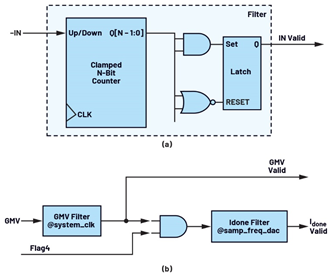
Figure 3b shows the proposed architecture implemented to declare that the battery is fully charged. The circuit consists of two FIR filters with different clocks and dimensions. Referring to Figure 1b, if the GMV signal is validated by the GMV filter, the charger moves to the constant voltage zone, and if the battery current is below the Idone threshold, the charging process can be considered complete and stopped. Note that in constant voltage mode (CV state in Figure 1a), the battery current may decrease for reasons other than the natural evolution of the system, such as thermal loop intervention or an increase in battery load. For this reason, it is important to also validate Flag4 through the Idone filter, which also senses the Idone signal. The filters have different sizes, given that the GMV signal is sampled by a clock that is usually the system clock—for example, a clock that is faster than the sampling rate of the ADC inside the microprocessor.
Simulation Results
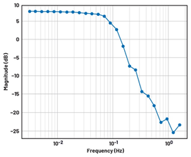
The proposed solution has been analyzed by estimating an empirical frequency response of the filter by exciting it with inputs whose probability of being 1 varies sinusoidally at a controlled frequency f (this directly sets the frequency of change of the binary input sequence). Figure 4 shows how the rate of change in the input signal affects the behavior of the saturated up/down counter filter used as a hardware approximation of a moving average filter. It is important to emphasize that, in this context, the term frequency does not refer to the system clock frequency (for example, how often samples are acquired), but to the frequency of change of the samples themselves—that is, how quickly the binary input sequence varies over time.
The filter under study increases or decreases its internal state by one unit at each sample, with saturation at zero and at an upper threshold. Under slow variation of the input—for example, when the signal exhibits a long run of consecutive 1s or 0s—the filter has enough time to raise or lower the counter to the thresholds, and the output faithfully reproduces the behavior expected from a moving average filter over an equivalent window. In this regime, the empirically measured frequency response shows a nearly constant gain at low frequencies, confirming that the filter preserves the input’s average information.
As the frequency of change of the input samples increases, the situation changes. If the signal alternates rapidly between 1 and 0, the counter can no longer reach the threshold value before the input changes direction again, preventing the filter from producing the same output that a moving average filter would. Consequently, the measured gain at the corresponding variation frequency drops significantly, indicating that the filter has lost the ability to follow rapid input changes.
The proposed circuit has been preliminarily validated by conducting a formal analysis using MATLAB, and its robustness has been tested using many different input sequences for GMV and Flag4 signals.
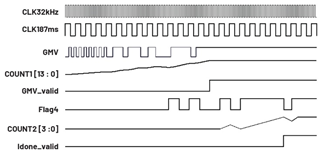
Hence, the designed circuit was synthesized using a 90nm technology and simulated standalone, also including the parasitic effects extracted from Innovus (place and route (PNR)) tool. Figure 5 shows typical GMV and Flag4 (Idone) behavior during the battery charging phase: initially, the GMV switches uncertainly and then becomes almost stable. Note that COUNT1 rises/falls as the GMV is high/low until GMV_valid is declared. With the traditional debouncing approach, when the last glitch occurs, the counter would have been reset, and the counting would have started over again, extending the constant-current charging time. Once the constant voltage zone is reached, the FSM waits for the Ibat to drop below the Idone value (Flag4), and this information is provided at a specific rate by the processor. This signal is also not always stable, so the filter monitors it for a precise time window during which the GMV must always confirm constant voltage operation. When COUNT2 expires, Idone_valid is given, and the charging process is concluded.
Observe the comparison in terms of area and memory elements between the buffer-based approach and the proposed one. Table 1 presents data extracted using the Genus tool. As shown, the area occupied by the memory-based solution grows exponentially with the number of averaged samples—a direct consequence of the filter needing to store more samples, which in turn increases the buffer size. Common integrated solutions often work with a 32kHz clock, which means the averaged samples in one second are 32,000, so the buffer should be composed of 32,000 flip-flops to store all the samples; that leads to a huge waste of area occupation. The proposed solution reduces the area occupied since it uses a counter to determine the number of ones/zeros in the last half-period and does not need to memorize all the samples. The key difference is that a unit increase in a sample involves the addition of a memory element in the classic solution, unlike the proposed solution, in which the number of flip-flops increases by one each time the number of samples increases by a power of 2.
Table 1. Area and Memory Elements Comparison
| N Flip-Flops Area (μm2) | ||||
| N Samples | Buffer | Proposed | Buffer | Proposed |
| 16 | 29 | 4 | 978 | 166 |
| 64 | 79 | 6 | 3024 | 263 |
| 256 | 281 | 8 | 10464 | 361 |
| 1024 | 1055 | 10 | 38469 | 456 |
Conclusion
A new filtering approach to validate an unstable analog signal has been presented. It consists of an up-down counter having two different saturation thresholds, which, under certain conditions, reproduces exactly the behavior of a moving average FIR filter. The results demonstrate the correct functionality of the filter, highlighting the limits if the frequency of change of the input sample increases. Indeed, the counter can no longer reach the threshold value before the input changes direction again, producing a different output in comparison to a classical moving average. The biggest advantage is the absence of a memory to retain all the previous samples to update the real-time average, removing the oldest sample from the observation window and introducing the new one. The key difference is that a unit increase in a sample involves the addition of a memory element in the classic solution, while in the proposed solution the number of flip-flops increases by one each time the number of samples increases by a power of 2. The filter was also used to correlate two analog signals with different frequencies, resulting in a more efficient way to detect the termination current of a battery charge, and it saves area because it does not use any additional memory to store the acquired samples. This circuit has been implemented into the charger for voltage mode detection (first analog signal) and termination current validation (second signal).
References
1Bruno Do Valle, Christian T. Wentz, and Rahul Sarpeshkar. “An Area and Power-Efficient Analog Li-Ion Battery Charger Circuit.” IEEE Transactions on Biomedical Circuits and Systems, Vol. 5, No. 2, April 2011.
2Chia-Hsiang Lin, Chun-Yu Hsieh, and Ke-Horng Chen. “A Li-Ion Battery Charger with Smooth Control Circuit and Built-In Resistance Compensator for Achieving Stable and Fast Charging.” IEEE Transactions on Circuits and Systems I: Regular Papers, Vol. 57, No. 2, February 2010.
3Shang-Hsien Yang, Jen-Wei Liu, and Chua-Chin Wang. “A Single-Chip 60-V Bulk Charger for Series Li-Ion Batteries with Smooth Charge-Mode Transition.” IEEE Transactions on Circuits and Systems I: Regular Papers, Vol. 59, No. 7, July 2012.
4Min Chen and Gabriel A. Rincon-Mora. “Accurate, Compact, and Power-Efficient Li-Ion Battery Charger Circuit.” IEEE Transactions on Circuits and Systems II: Express Briefs, Vol. 53, No. 11, November 2006.
5Chia-Chun Tsai, Chin-Yen Lin, Yuh-Shyan Hwang, Wen-Ta Lee, and Trong-Yen Lee. “A Multi-Mode LDO-Based Li-Ion Battery Charger in 0.35/spl mu/m CMOS Technology.” The 2004 IEEE Asia-Pacific Conference on Circuits and Systems, 2004.
6Chia-Hsiang Lin, Chi-Lin Chen, Yu-Huei Lee, Shih-Jung Wang, Chun-Yu Hsieh, and Hong-Wei Huang. “Fast Charging Technique for Li-Ion Battery Charger.” IEEE International Conference on Electronics, Circuits and Systems, 2008.
7Ivan Porcelli, Marco Masini, Gianluca Belluco, and Manuel Di Cera. “A Compact Polling Strategy to Accurately Detect Li-Ion Battery Termination Current Saving Die Area.” ADI Italian Technology Conference, 2025.
8Nan-Hsiung Tseng, Chun-Yuan Chen, Fu-Heng Chen, Yu-Tse Shih, Li-Jen Huang, and Ming-Che Tu. “A 97.1%-Efficient Buck–Boost Battery Charger With Constant Current Extension and Precision-Adjustable Current Monitoring for 2× Faster Battery Charging.” IEEE Transactions on Power Electronics, Vol. 41, No. 2, February 2026.
9Ruei-Hong Peng, Tsu-Wei Tsai, Ke-Horng Chen, Zhih Han Tai, Yi Hsuan Cheng, and Chi Chung Tsai. “Switching-Based Charger with Continuously Built-In Resistor Detector (CBIRD) and Analog Multiplication-Division Unit (AMDU) for Fast Charging in Li-Ion Battery.” Proceedings of the IEEE European Solid-State Circuits, 2013.
10Tzu-Chi Huang, Ruei-Hong Peng, Tsu-Wei Tsai, Ke-Horng Chen, and Chin-Long Wey. “Fast Charging and High-Efficiency Switching-Based Charger with Continuous Built-In Resistance Detection and Automatic Energy Deliver Control for Portable Electronics.” IEEE Journal of Solid-State Circuits, Vol. 49, No. 7, July 2014.
11Young-Ho Jung, Jae-Hyung Jung, Hoe-Eung Jeong, Jae-Hoon Jung, Jae-Sung An, and Hyun-A. Ahn. “A Fast and Highly Accurate Battery Charger with Accurate Built-In Resistance Detection.” IEEE Transactions on Power Electronics, Vol. 33, No. 12, December 2018.
12Maurice Bellanger and Benjamin A. Engel. “Finite Impulse Response (FIR) Filters.” Digital Signal Processing: Theory and Practice, 2024.
About the Authors
Alessandro Pidatella is a digital design engineer at Analog Devices, working in the Healthcare VSMIC and PMIC group in Catania, Italy. His work focuses on the design and integration of digital architectures for complex mixed-signal systems, with emphasis on power management ICs for advanced healthcare applications. He is involved in the development of control logic, finite state machines, and system-level digital solutions, supporting the interaction between digital and analog domains in highly integrated environments. His contributions span from architecture definition to implementation and verification, with a strong focus on robustness, power efficiency, and system optimization.
Rosario Mita is a staff digital design engineer at Analog Devices. He received his Ph.D. degree in electrical engineering from the University of Catania, Italy. He has more than 25 years of experience spanning academic research and industrial R&D in digital, analog, and mixed-signal design. His expertise includes advanced digital architectures, FPGA-based systems, and circuit/system modeling. At ADI, he focuses on asynchronous digital design and the development of robust architectures for complex systems. He is a co-inventor on three patents and the author or co-author of more than 50 peer-reviewed international publications in leading journals and conference proceedings.
Angelo Mazzone is a director of the Mixed-Signal Design Engineering Group at Analog Devices, with extensive experience in the design and development of complex integrated systems for power management and healthcare applications. He leads a multidisciplinary team within the Healthcare VSMIC and PMIC organization, driving the architecture and execution of advanced mixed-signal solutions. Based in Italy, he has played a key role in the definition and delivery of highly integrated power management ICs, contributing to system-level architecture, cross-functional coordination, and project execution from specification through tape-out. In his role, Angelo is actively involved in technical decision-making, project reviews, and alignment across design teams, ensuring robust and scalable solutions. His work spans digital and analog domains, with a strong focus on system integration, power efficiency, and design optimization for complex applications.