

The global semiconductor process control equipment market is entering a high-growth phase as chip manufacturers race toward 2nm-class technologies, AI accelerators, high-bandwidth memory (HBM), advanced packaging and increasingly complex transistor architectures. As semiconductor geometries shrink, even microscopic defects or process variations can significantly reduce yield, making inspection, metrology and automated process control essential to modern chip manufacturing.
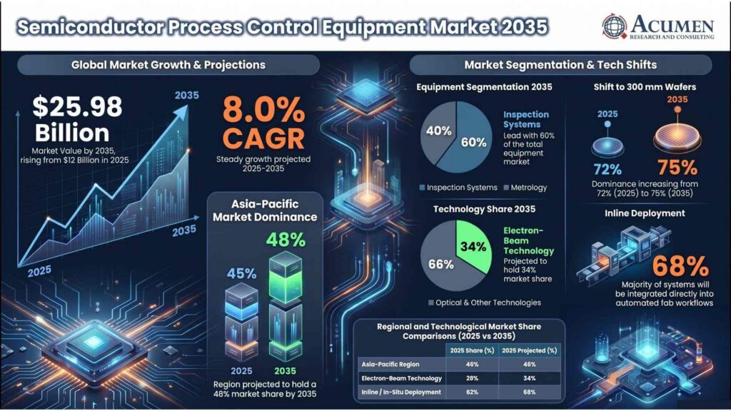
According to Acumen Research and Consulting, the Semiconductor Process Control Equipment Market size was valued at USD 12 billion in 2025 and is projected to reach USD 25.98 billion by 2035, expanding at a CAGR of 8.0% from 2026 to 2035.
Semiconductor Process Control Equipment Market Overview
Semiconductor process control equipment comprises inspection, metrology, defect review and analysis technologies used to monitor manufacturing processes, identify defects and maintain consistent production quality. These systems help semiconductor manufacturers measure critical dimensions, overlay, film thickness, pattern accuracy, surface quality and other parameters throughout wafer fabrication and packaging.
The rapid transition toward advanced semiconductor nodes is increasing the importance of process control. Manufacturing at 3nm, 2nm and below involves tighter process windows and more complicated device structures, including gate-all-around (GAA) transistors. At the same time, AI processors and HBM require sophisticated manufacturing and packaging processes, creating additional inspection and measurement requirements.
The broader semiconductor equipment industry also reflects this momentum. Global semiconductor equipment billings reached $135.1 billion in 2025, up 15% from $117.1 billion in 2024. Wafer-processing equipment increased 12%, while test-equipment billings surged 55%, highlighting growing requirements for inspection, measurement and testing associated with AI and HBM production.
What Is Driving the Semiconductor Process Control Equipment Market?
The biggest growth catalyst is the increasing complexity of semiconductor manufacturing.
AI accelerators, high-performance computing chips and advanced memory devices require sophisticated manufacturing processes. More process steps mean more opportunities for defects and process variation. Consequently, fabs are increasing inspection points and deploying increasingly automated metrology and process-control systems.
The move to 2nm semiconductor manufacturing is another major opportunity. Smaller features and GAA architectures require tighter control of critical dimensions, overlay, materials and pattern defects. Electron-beam inspection and advanced optical metrology are becoming increasingly important for detecting problems that conventional approaches may miss.
Advanced packaging is also expanding the addressable market. Chiplet architectures, heterogeneous integration and high-density interconnects introduce additional requirements for inspection and measurement beyond conventional front-end wafer fabrication.
The Acumen Research And Consulting report identifies AI-driven manufacturing, advanced packaging, HBM and semiconductor localization as major opportunities for process-control suppliers.
Semiconductor Process Control Equipment Market Statistics and Key Trends
Several statistics highlight the structure of the market:
- The global market was $12 billion in 2025 and is forecast to reach $25.98 billion by 2035.
- The market is projected to grow at an 8.0% CAGR during 2026–2035.
- Asia-Pacific held 45% of the global market in 2025 and is expected to reach 48% by 2035.
- North America accounted for 28.5% of the market in 2025.
- Inspection systems represented 60% of the equipment-type market in 2025.
- Metrology systems held 33%.
- Optical-based technologies accounted for 58%, while electron-beam-based technologies represented 29%.
- 300mm wafers accounted for 72% of the market in 2025.
- Pure-play foundries represented the largest end-user segment at 38%.
- Front-end-of-line (FEOL) applications held 55% of the market.
- Inline/in-situ deployment accounted for 62% and is projected to reach 68% by 2035.
These figures indicate that high-volume advanced-node manufacturing remains the core demand center, while advanced packaging and real-time process monitoring are creating additional growth avenues.
For companies, investors and semiconductor manufacturers seeking detailed forecasts, segmentation and regional analysis, the complete sample pages of Semiconductor Process Control Equipment Market report provides comprehensive market intelligence through 2035.
Which Segment Dominates the Semiconductor Process Control Equipment Market?
Inspection Systems Lead Equipment Demand
Inspection systems dominated the semiconductor process control equipment market with a 60% share in 2025. These systems identify particles, contamination, pattern defects, surface imperfections and other manufacturing deviations.
The economic impact of defects increases dramatically as chip geometries become smaller. A defect that might have been manageable on an older process node can become a yield-limiting problem on an advanced node. This makes high-throughput, high-resolution inspection increasingly valuable.
Metrology systems ranked second with a 33% share. They measure parameters such as critical dimensions, layer thickness, overlay and other process characteristics. Their importance is increasing alongside GAA transistors, 3D NAND and sophisticated advanced-packaging architectures.
Why Is Optical Inspection Important in Semiconductor Manufacturing?
Optical-based technology accounted for 58% of the semiconductor process control equipment market in 2025, making it the leading technology category.
Optical inspection is particularly attractive for high-volume semiconductor fabs because it combines speed and throughput with the ability to inspect large wafer areas. However, increasingly small defects are creating demand for higher-resolution technologies.
Electron-beam-based systems accounted for 29% in 2025 and are projected to increase to 34% by 2035. Their ability to identify and analyze extremely small defects makes e-beam inspection particularly relevant to advanced semiconductor nodes.
How Is AI Changing Semiconductor Process Control?
Artificial intelligence is transforming semiconductor process control from conventional defect detection into predictive and data-driven manufacturing.
Modern fabs generate enormous quantities of data from inspection tools, metrology systems, sensors and manufacturing equipment. AI and machine learning can correlate this information to identify patterns, classify defects and detect potential yield excursions.
Applied Materials has previously highlighted the integration of optical inspection, e-beam review, big data and AI to distinguish yield-critical defects from nuisance signals. Its process-control approach illustrates the industry’s shift toward intelligent inspection and real-time process optimization.
The significance of AI is therefore twofold: AI is increasing demand for complex chips while simultaneously becoming a technology used to manufacture those chips more efficiently.
Why Is Asia-Pacific the Largest Semiconductor Process Control Equipment Market?
Asia-Pacific dominated the global market with a 45% share in 2025, and its share is projected to increase to 48% by 2035. The regional market is expected to grow from approximately $5.87 billion in 2026 to $12.47 billion in 2035, representing an 8.7% CAGR.
Taiwan, South Korea, China and Japan form the center of the region’s semiconductor manufacturing ecosystem. The concentration of foundries, memory manufacturers, IDMs, equipment suppliers and advanced packaging facilities creates sustained demand for process control.
China spent approximately $49.3 billion on semiconductor equipment in 2025, while Taiwan’s equipment spending reached $31.5 billion after increasing 90% year over year. South Korea spent $25.8 billion, up 26%, driven substantially by HBM and DRAM investment.
India is also emerging as a new opportunity. Acumen reports 12 approved semiconductor manufacturing units with cumulative investment exceeding ₹1.64 lakh crore, creating future demand for inspection, metrology, testing and quality-control equipment.
What Are the Latest Developments Among Semiconductor Process Control Equipment Companies?
Competition is increasingly centered on higher resolution, AI-enabled inspection, advanced metrology and integrated process-control platforms.
KLA Corporation remains one of the most significant players in semiconductor process control. Its fiscal 2026 semiconductor process-control revenue increased 12%, supported by foundry/logic and memory investment related to AI and HPC, as well as adoption of advanced-packaging products.
KLA also expanded its presence in India. According to Acumen Research and Consulting, the company inaugurated a ₹300 crore R&D facility in Chennai in January 2026, covering approximately 3.11 lakh square feet and designed to accommodate up to 1,300 employees.
Onto Innovation has pursued an especially aggressive expansion strategy. In 2025, the company agreed to acquire Semilab International’s materials analysis business in a transaction valued at approximately $545 million, adding technologies for materials characterization, contamination monitoring and advanced semiconductor applications.
In April 2026, Onto announced another major strategic investment: an agreement to acquire a 27% stake in Rigaku for approximately $710 million. The investment is intended to strengthen collaboration in X-ray-based process control for advanced logic and memory applications.
Other important market participants include ASML, Hitachi High-Tech, Lasertec, Nova, Tokyo Electron, Thermo Fisher Scientific and Camtek, with companies targeting different portions of inspection, metrology, materials analysis, advanced packaging and defect-review applications.
What Are the Key Opportunities in the Semiconductor Process Control Equipment Market?
The strongest opportunities are emerging at the intersection of AI chips, advanced memory and advanced packaging.
The continued construction of semiconductor fabs creates a direct opportunity for process-control suppliers. At the same time, upgrading existing fabs with newer inspection and metrology technologies can generate replacement demand.
Advanced packaging is particularly significant because chiplets and heterogeneous integration introduce complex structures that must be measured and inspected at multiple stages.
The growing importance of HBM and advanced DRAM is another major opportunity. As memory architectures become more sophisticated, manufacturers require tighter control over dimensions, defects and materials.
Geographic diversification is also expanding the addressable market. Government incentives in the United States, India, South Korea, Japan and other countries are encouraging local semiconductor production, potentially creating new demand for process-control infrastructure.
What Are the Challenges Facing the Semiconductor Process Control Equipment Market?
The primary challenge is the high cost and technical complexity of advanced inspection and metrology systems. Semiconductor manufacturers must justify significant capital expenditure while maintaining high equipment utilization and return on investment.
Export controls and geopolitical tensions represent another uncertainty. Restrictions on advanced semiconductor equipment can influence purchasing decisions, supply chains and technology development.
At the same time, semiconductor manufacturers increasingly expect process-control suppliers to integrate hardware, software, analytics and automation rather than provide standalone measurement equipment.
Frequently Asked Questions About the Semiconductor Process Control Equipment Market
How big is the semiconductor process control equipment market?
The global semiconductor process control equipment market size reached $12 billion in 2025 and is projected to reach $25.98 billion by 2035, according to Acumen Research and Consulting.
What is the CAGR of the semiconductor process control equipment market?
The global semiconductor process control equipment market is projected to grow at a CAGR of 8.0% between 2026 and 2035.
Which region dominates the semiconductor process control equipment market?
Asia-Pacific is the leading regional market, accounting for 45% of global revenue in 2025. Its share is expected to increase to 48% by 2035, supported by semiconductor manufacturing investments across Taiwan, South Korea, China and Japan.
Which companies are leading the semiconductor process control equipment market?
Key companies include KLA Corporation, ASML Holding, Hitachi High-Tech, Onto Innovation, Lasertec, Nova, Tokyo Electron, Thermo Fisher Scientific and Camtek. These companies compete across inspection, metrology, defect review, materials analysis and advanced packaging process-control technologies.
What is semiconductor process control equipment used for?
Semiconductor process control equipment is used to inspect wafers and semiconductor structures, measure critical dimensions and process parameters, identify defects, analyze materials and provide manufacturing feedback. These capabilities help fabs improve yield, maintain process uniformity and reduce manufacturing variability.
Why is semiconductor inspection important for advanced chips?
Advanced semiconductor manufacturing involves extremely small structures and increasingly narrow process tolerances. High-resolution inspection helps manufacturers identify defects and process deviations before they cause significant yield losses, making inspection essential for 3nm, 2nm, advanced memory and complex packaging production.
What is the future outlook for semiconductor process control equipment?
The outlook remains positive as semiconductor manufacturers invest in AI processors, HBM, advanced logic, 2nm-class technologies and advanced packaging. The increasing integration of AI, automation and real-time analytics should further shift process control from periodic inspection toward continuous, intelligent manufacturing optimization.
Final Outlook: A Critical Market for the AI Semiconductor Era
The semiconductor process control equipment market is becoming one of the most strategically important segments of the semiconductor equipment industry. The transition to 2nm and beyond, rising AI-chip production, HBM expansion, advanced packaging and semiconductor localization are all increasing the need to detect defects and control manufacturing processes with greater precision.
With the market projected to more than double from $12 billion in 2025 to $25.98 billion by 2035, process control is positioned to benefit from semiconductor industry’s ongoing technology transition.
For detailed market sizing, competitive analysis, segmentation by equipment type, technology, wafer size, end user, manufacturing application and deployment configuration, readers can explore the complete Semiconductor Process Control Equipment Market report.
Businesses evaluating this market can also request the sample pages of the Semiconductor Process Control Equipment Market report to review the research scope, methodology and detailed market coverage.